RL78/F13, F14 CHAPTER 17 LIN/UART MODULE (RLIN3)
R01UH0368EJ0210 Rev.2.10 1239
Dec 10, 2015
If it is necessary to set the URDCC bit in the LUSCn register to 1 (comparison of received data and LIDBn register data
enabled in SNOOZE mode), only use SNOOZE mode with the UBLS bit in the LBFCn register set to 0 (UART 8-bit character
communication) and UEBE bit in the LUORn1 register set to 0 (expansion bit operation disabled).
17.5.2 Data Transmission/Reception
(1) Data Transmission
One bit of data is transmitted per Tbit.
In half-duplex communication, if the BERE bit in the LEDEn register is 1 (bit error detection enabled), the transmission data
and the input pin level are compared bit by bit during data transmission, and the results are stored in the BER flag in the
LESTn register (see 17.5.5 Error Status). The timing at which the input pin is sampled during data transmission can vary
depending upon the settings of the LPRS[2:0] and NSPB[3:0] bits in the LWBRn register.
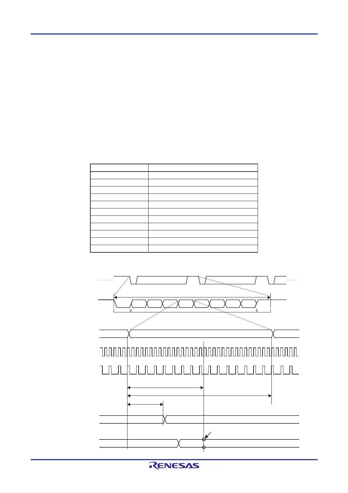
The bit error detection timing in UART mode is shown in Table 17-25.
Table 17-25. Error Detection Timing in UART Mode
Sampling count per bit Bit error detection timing
6 samples 3rd clock cycle + one cycle of the prescaler clock
7 samples 4th clock cycle + one cycle of the prescaler clock
8 samples 4th clock cycle + one cycle of the prescaler clock
9 samples 5th clock cycle + one cycle of the prescaler clock
10 samples 5th clock cycle + one cycle of the prescaler clock
11 samples 6th clock cycle + one cycle of the prescaler clock
12 samples 6th clock cycle + one cycle of the prescaler clock
13 samples 7th clock cycle + one cycle of the prescaler clock
14 samples 7th clock cycle + one cycle of the prescaler clock
15 samples 8th clock cycle + one cycle of the prescaler clock
16 samples 8th clock cycle + one cycle of the prescaler clock
Figure 17-36. Example of Data Transmission Timing (when Sampling Count is 16 in 1 Tbit)
ST
SPST
SP ST SP
D0 D1 D2 D3 D4 D5 D6 D7
1 Tbit = 16 f
LIN
Synchronization LRXDn
(Internal signal)
Data (8 bits) Data (8 bits)
Byte field
Stop bitData (8 bits)Start bit
Bit 3
Prescaler clock
(internal signal)
n = 0, 1
Physical layer
delay
Bit 3
LRXDn
Bit 3
Sampling point for bit error
detection
Sampling point for bit error detection
(8th clock cycle + 1 prescaler clock cycle)
f
LIN
(internal signal)
LTXDn
LTXDn
LTXDn
 Loading...


