RL78/F13, F14 CHAPTER 35 ELECTRICAL SPECIFICATIONS (GRADE K)
R01UH0368EJ0210 Rev.2.10 1772
Dec 10, 2015
35.6 Analog Characteristics
35.6.1
A/D Converter Characteristics
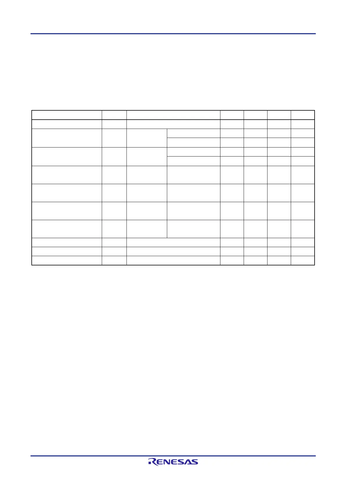
(1) When AVREF (+) = AVREFP/ANI0 (ADREFP1 = 0, ADREFP0 = 1), AVREF (-) = AVREFM/ANI1 (ADREFM = 1), target ANI
pin: ANI2 to ANI23 (power supply: V
DD)
(TA = -40 to +125C, 2.7 V EVDD0 = EVDD1 = VDD 5.5 V, VSS = EVSS0 = EVSS1 = 0 V, Reference voltage (+) = AVREFP,
Reference voltage (-) = AV
REFM = 0 V)
Parameter Symbol Conditions MIN. TYP. MAX. Unit
Resolution RES 8 10 bit
Overall error
Note 1
AINL 10-bit resolution
AV
REFP = VDD
4.0 V V
DD 5.5 V 1.2 3.0 LSB
2.7 V VDD < 4.0 V 1.2 3.5 LSB
Conversion time tCONV
10-bit resolution
AV
REFP = VDD
4.0 V V
DD 5.5 V 2.125 39
µs
2.7 V VDD < 4.0 V 3.1875 39
µs
Zero-scale error
Notes 1, 2
EZS
10-bit resolution
AV
REFP = VDD
2.7 V V
DD 5.5 V 0.25 %FSR
Full-scale error
Notes 1, 2
EFS
10-bit resolution
AV
REFP = VDD
2.7 V V
DD 5.5 V 0.25 %FSR
Integral linearity error
Note 1
ILE
10-bit resolution
AV
REFP = VDD
2.7 V V
DD 5.5 V 2.5 LSB
Differential linearity error
Note 1
DLE
10-bit resolution
AV
REFP = VDD
2.7 V V
DD 5.5 V 1.5 LSB
Reference voltage (+) AVREFP 2.7 VDD V
Analog input voltage VAIN 0 AVREFP V
Internal reference voltage (+) VBGR 2.7 V VDD 5.5 V 1.38 1.45 1.5 V
Notes 1. Excludes quantization error (1/2 LSB).
2. This value is indicated as a ratio (%FSR) to the full-scale value.
 Loading...


