RL78/F13, F14 CHAPTER 34 ELECTRICAL SPECIFICATIONS (GRADE L)
R01UH0368EJ0210 Rev.2.10 1684
Dec 10, 2015
34.2.3 Subsystem Clock Oscillator Characteristics
(TA = -40 to +105C, 2.7 V EVDD0 = EVDD1 = VDD 5.5 V, VSS = EVSS0 = EVSS1 = 0 V)
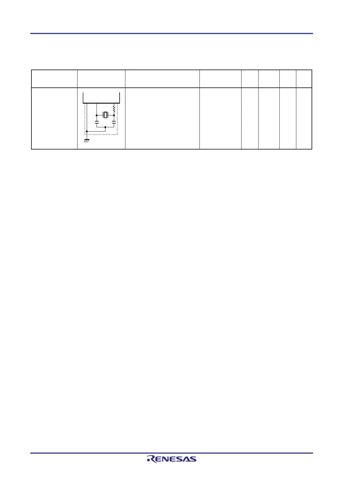
Resonator Recommended
Circuit
Item Conditions MIN. TYP. MAX. Unit
Crystal resonator
XT1 clock oscillation frequency
(fXT)
2.7 V VDD 5.5 V 29.0 32.768 35.0 kHz
Cautions 1. When using the XT1 oscillator, wire as follows in the area enclosed by the broken lines in the
above figures to avoid an adverse effect from wiring capacitance.
Keep the wiring length as short as possible.
Do not cross the wiring with the other signal lines.
Do not route the wiring near a signal line through which a high fluctuating current flows.
Always make the ground point of the oscillator capacitor the same potential as V
SS.
Do not ground the capacitor to a ground pattern through which a high current flows.
Do not fetch signals from the oscillator.
2.
The XT1 oscillator is designed as a low-amplitude circuit for reducing power
consumption and thus required to be adequately evaluated on the system. Customers
are requested to consult the resonator manufacturer to select an appropriate resonator
and to determine the proper oscillation constant.
C3
XT2XT1
C4
V
SS
Rd
 Loading...


