RL78/F13, F14 CHAPTER 34 ELECTRICAL SPECIFICATIONS (GRADE L)
R01UH0368EJ0210 Rev.2.10 1697
Dec 10, 2015
34.4 AC Characteristics
34.4.1 Basic Operation
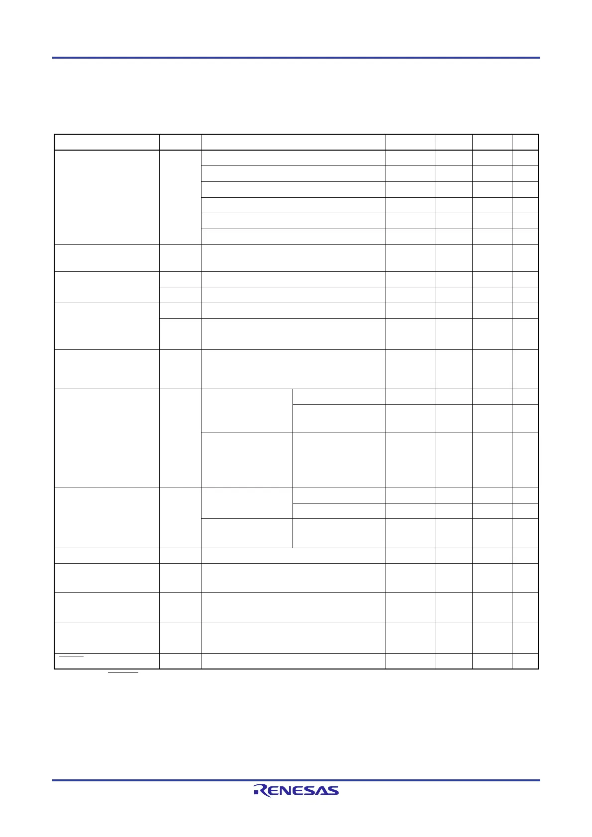
(TA = -40 to +105C, 2.7 V EVDD0 = EVDD1 = VDD 5.5 V, VSS = EVSS0 = EVSS1 = 0 V) (1/2)
Parameter Symbol Conditions MIN. TYP. MAX. Unit
Instruction cycle (minimum
instruction execution time)
T
CY High-speed on-chip oscillator clock operation 0.03125 1 s
High-speed system clock operation 0.05 1 s
PLL clock operation 0.03125 1 s
Subsystem clock operation 28.5 30.5 34.5 s
Low-speed on-chip oscillator clock operation 66.6 s
In self programming mode 0.03125 1 s
CPU/peripheral hardware
clock frequency
f
CLK 0.03125 66.6 s
External system clock
frequency
f
EX 1.0 20.0 MHz
fEXS 29 35 kHz
External system clock input
high-level width, low-level
width
t
EXH, tEXL 24 ns
tEXHS,
t
EXLS
13.7 s
TI00 to TI07, TI10 to TI17
input high-level width, low-
level width
t
TIH,
t
TIL
1/f
MCK
+10 ns
TO00 to TO07, TO10 to
TO17 output frequency
f
TO All TO pins,
Normal slew rate,
C = 30 pF
4.0 V EVDD0 5.5 V
16 MHz
2.7 V EVDD0 < 4.0 V
8 MHz
TO01, TO06, TO07,
TO11, TO13 only,
Special slew rate,
C = 30 pF
2 MHz
PCLBUZ0 output frequency fPCL Normal slew rate
C = 30 pF
4.0 V EVDD0 5.5 V
16
MHz
2.7 V EVDD0 < 4.0 V
8
MHz
Special slew rate
C = 30 pF
2
MHz
Timer RJ input cycle tC TRJIO0 100 ns
Timer RJ input high-level
width, low-level width
t
WH,
t
WL
TRJIO0 40 ns
Interrupt input high-level
width, low-level width
t
INTH,
t
INTL
INTP0 to INTP13
Note
1 s
KR0 to KR7 key interrupt
tinput low-level width
t
KR 250 ns
RESET low-level width tRSL 10 s
Note Pins RESET, INTP0 to INTP3, INTP12, and INTP13 have noise filters for transient levels lasting less than 100 ns.
Caution Excluding the error in oscillation frequency accuracy.
Remark f
MCK: Timer array unit operation clock frequency
<R>
 Loading...


