Memory Interface Routing
R
Intel
®
Pentium
®
4 Processor / Intel
®
850 Chipset Family Platform Design Guide 101
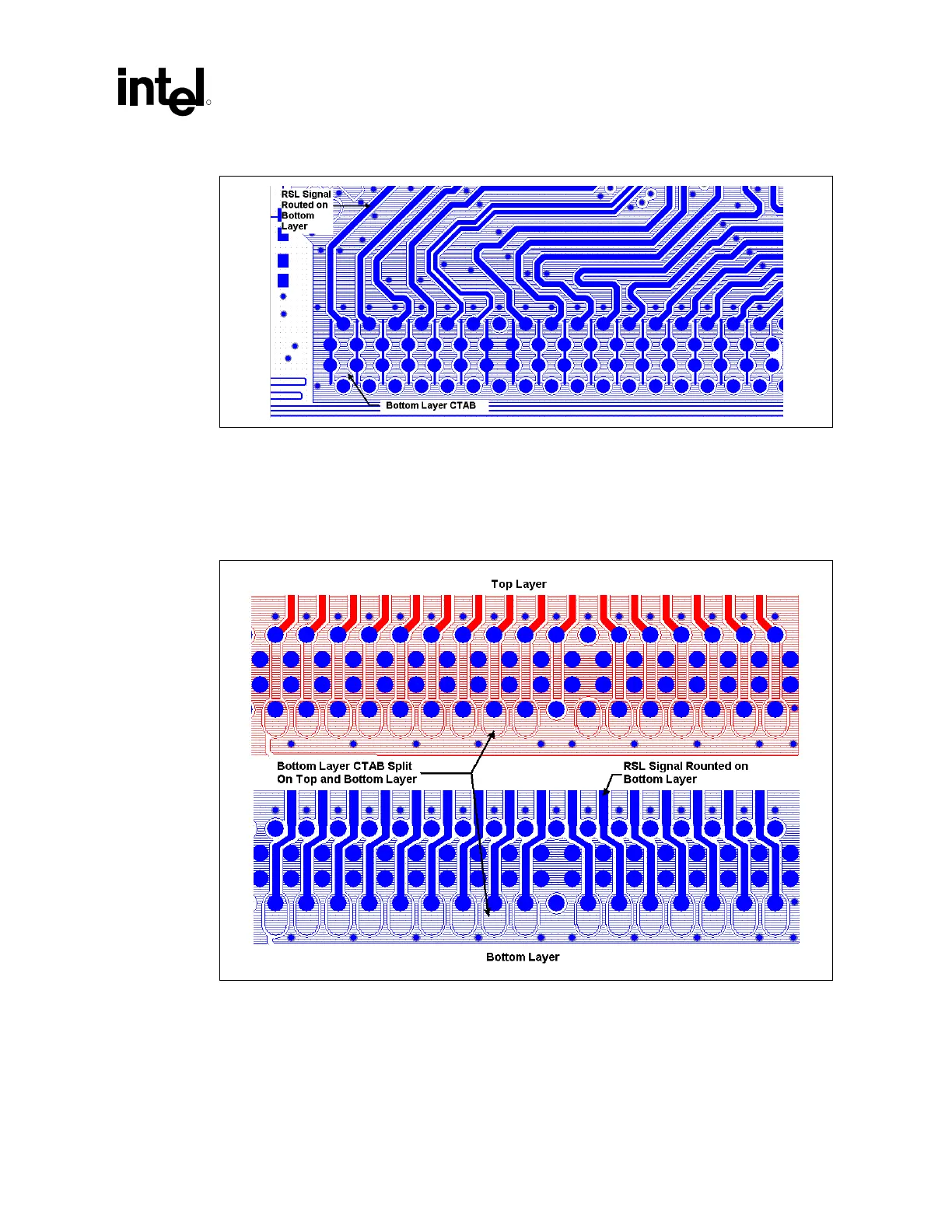
Figure 63. Bottom Layer CTAB with RSL Signal Routed on the Same Layer (Ceff = 1.35 pF)
The CTAB can be implemented on the multiple layers to minimize routing and space constrains.
Figure 64 issues the use of CTABs on the top and bottom layer for bottom layer RSL and clocking
signals routed between RIMM connectors.
Figure 64. Bottom Layer CTABs Split Across the Top and Bottom Layer to Achieve an Effect
Ceff ~1.35 pF
 Loading...

