Schematic Review Checklist
R
Intel
®
Pentium
®
4 Processor / Intel
®
850 Chipset Family Platform Design Guide 251
15.4 Intel
®
850 Chipset Checklist
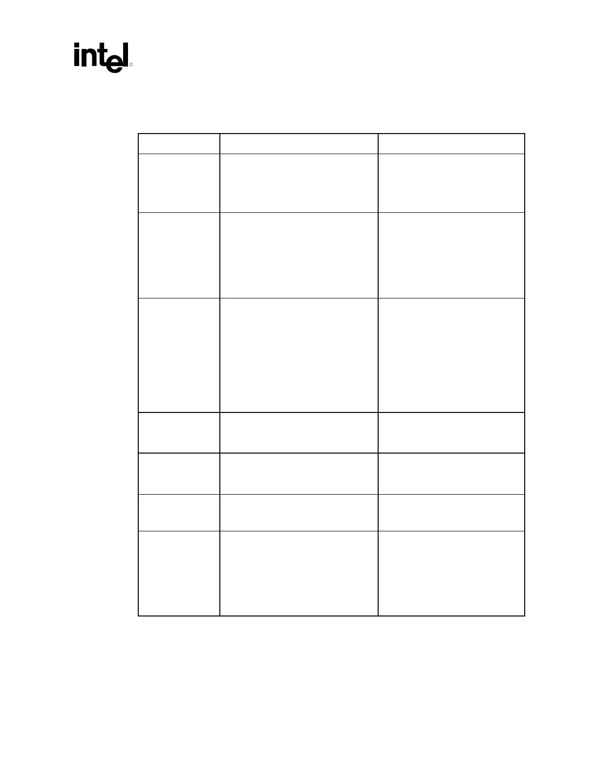
Checklist Items Recommendations Reason/Impact
HL_STB
HL_STB#
• Connect to ICH2 • The length of both hub interface
strobe signals must be matched
within ±0.1 inches of the HL_STB
differential pair.
• Refer to Section 8.2.1.
HDVREF[3:0]
HAVREF[3:0]
CCVREF
• Connect voltage divider to pins.
50
Ω ±1% pull-up to VCC and
100
Ω ±1% pull-down resistor to GND.
• Decouple the voltage divider with a 1 µf
capacitor.
• Keep the voltage divider within
1.5 inches of the MCH V
REF
ball.
• A single reference divider circuit for
all signals is considered sufficient.
• Refer to Section 5.5.
HUBREF • Use a voltage divider circuit with
R1=R2=150
Ω ±1%
• The reference voltage generated by a
single HUBREF divider should be
bypassed to ground at each
component with a 0.01
µF capacitor
located close to the component (MCH
and ICH2) HUBREF pin. Decouple the
voltage divider circuit with a 0.1 µF
capacitor placed near the voltage
divider circuit.
• Refer to Section 8.2.3.
GRCOMP • Must be tied to a 40 Ω ±2% or
39
Ω ±1% pull-down resistor to ground.
• Connect within 0.5 inches of the
ball.
• Refer to Section 7.1.8.
HLR_COMP • RCOMP Resistor tied to VSS:
• Normal: 40 Ω ±2% or 39 Ω ±1% with a
trace impedance of 60
Ω ±15%.
• Refer to Section 8.2.4.
HR_COMP • Use 20.75 Ω ±1% pull-down to VSS • Refer Section 5.5.
HSWNG [1:0] • Connect voltage divider to pins. 150 Ω
pull-down to GND and a 301
Ω pull-up
resistor to V
TT
.
• Decouple the voltage divider with a 1 µf
capacitor.
• Keep the voltage divider within
1.5 inches of the MCH V
REF
ball.
• Refer to Section 5.5.
 Loading...

