Memory Interface Routing
R
94 Intel
®
Pentium
®
4 Processor / Intel
®
850 Chipset Family Platform Design Guide
6.1.2 Rambus* Signaling Level (RSL) Channel Compensation
The RSL and clocking signals require special compensation for any discontinuities introduced in
the channel. Since the Direct Rambus channel only allows for 125ps of interconnect skew, it is
critical to minimize skew and to match the skew on RSL and clocking signals within a given
channel. The next few sections will show how to compensate for skew due to package trace
differences, vias, differential clock routing and connector.
When compensating a channel, the compensating techniques must be performed in the following
layout order:
1. Package trace compensation
2. Via compensation
3. Differential clock compensation
4. Alternating signal layer for RIMM connector pin compensation
5. RIMM connector impedance compensation
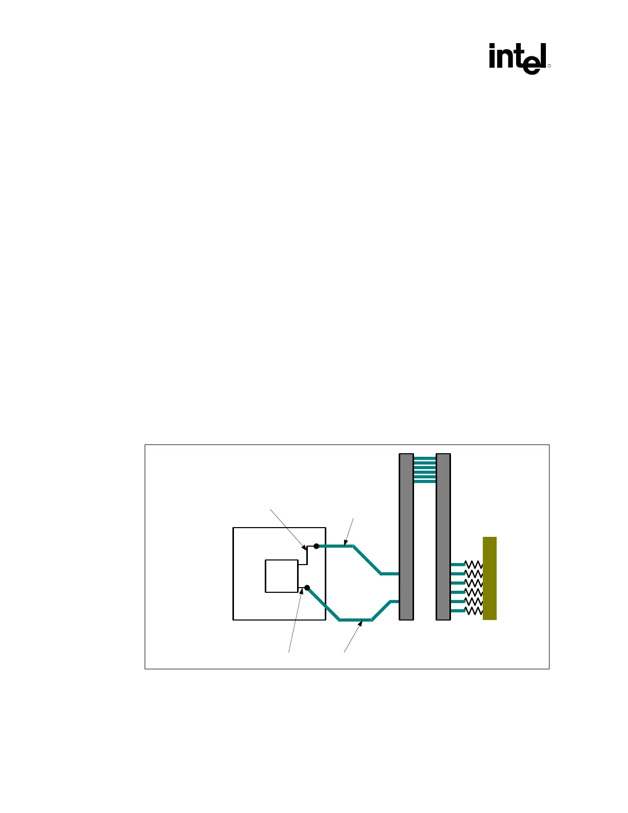
6.1.2.1 Package Trace Compensation (RSL and Clocking Signals)
All RSL and clocking signals require pad-to-pin length matching between the MCH to the first
RIMM connector to minimize skew. All RSL and clocking signals for a given channel required
pad-to-pin trace matching within ±10 mils.
The RIMM connector to RIMM connector trace length match requirement is ±2 mils.
Figure 59. Direct Rambus Channel Trace Length Matching Example
MCH
Package
MCH
Die
RIMM Connector
V
T
E
R
M
L1
L2
L3
L4
RIMM Connector
NOTE: This diagram only illustrates the routing of one Direct Rambus channel. However, the example routing
shown can be applied to both channels.
 Loading...

