Schematic Review Checklist
R
Intel
®
Pentium
®
4 Processor / Intel
®
850 Chipset Family Platform Design Guide 255
15.6 Rambus RIMM* Connector Checklist
Note:
• S3 (Suspend To RAM):
RDRAM device support Æ 2.5 V (ON), 1.8 V (ON), 3.3 V (N/A)
• S5 – 2.5 V (OFF), 1.8 V (OFF), 3.3 V (OFF)
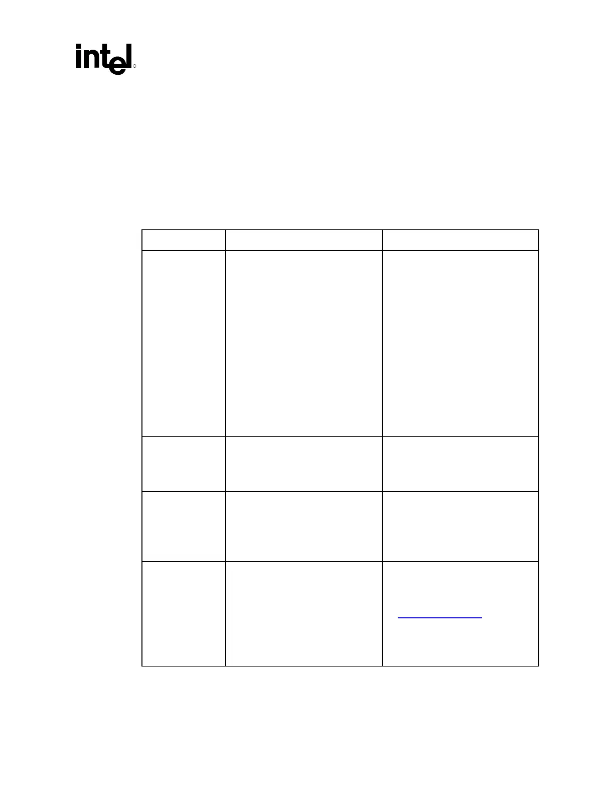
Checklist Items Recommendations Reason/Impact
LCTM, LCTM#
RCTM, RCTM#
LCFM, LCFM#
RCFM, RCFM#
LROW[2:0]
RROW[2:0]
LCOL[4:0]
RCOL[4:0]
RDQA[8:0]
LDQA[8:0]
RDQB[8:0]
LDQB[8:0]
CMD
SCK
• 0.8 pF – 1.35 pF compensating
capacitance is required on each of
these RSL connector pins.
• The RIMM* connector pin inductance
has been shown to cause an
impedance discontinuity on the
Rambus channel. This may reduce
voltage and timing margin.
• Above are examples of calculated
numbers. Actual calculated values
may vary with board variations. Use
CTAB calculations for specific
values.
• Refer to Section 6.1.2.5.
RSL Signal
Termination
• All RSL signals must be terminated to
1.8 V (V
TERM
) using 27 Ω 1% or
28
Ω 2% tolerance resistors at the
end of the channel opposite the
MCH.
• Rpacks are OK.
• Refer to Section 6.1.3.
RC Termination • Due to the buffer strengths in the
MCH, the high-speed CMOS signals
require DC termination.
• Terminate with 91 Ω ±2% pull-up and
a 39
Ω ±2% pull-down resistor to
ensure proper resuming from S3.
• The MCH tri-states SCK during STR
entry causing a glitch on SCK.
• Refer to Section 6.1.5.
SVDD (A56 and
B56)
• Should be tied to 3.3 V for EEPROM
(SPD) on RIMM modules.
• If the SMBus is tied to 3.3V
SB
, then
either:
Provide proper isolation on
SCL /SDA and pull SVDD to 3.3 V
OR
Tie SVDD to 3.3V
SB
.
• Ensure proper isolation if some
SMBUS devices are powered by
3.3V
SB
.
• Refer to the RAMBUS datasheets at
http://www.rambus.com
 Loading...

