Memory Interface Routing
R
108 Intel
®
Pentium
®
4 Processor / Intel
®
850 Chipset Family Platform Design Guide
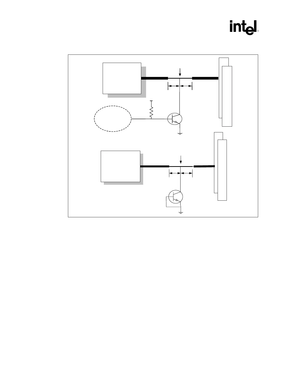
Figure 71. Rambus RDRAM* Device CMOS Shunt Transistor
R
I
M
M
S
SCK
MCH
175
mils
175
mils
5 mils
wide
MCH
R
I
M
M
S
5 mils
wide
175
mils
175
mils
CMD
2N3904
R
5V
Q
Control
Logic
This implementation is applicable for RIMM connectors down solution only and is not needed on
the repeater channels. Also, this implementation is not necessary if Suspend-to-RAM is not
supported within the system
6.1.8 Rambus RDRAM* Device Channel Margin Improvement
For Intel 850E / 533 MHz (PC1066) RDRAM device designs which exhibit less than optimum
Rambus channel margins, margin improvement may be achieved by:
• Increasing the number of bypass capacitors from one 0.1µF ceramic chips capacitors per two
RSL lines to two 0.1µF ceramic chip capacitors per two RSL lines. See Section 6.1.3.
• Insuring that the RIMM module with the most number of RDRAM devices is placed in the #1
RIMM connector.
 Loading...

