System Bus Routing
R
74 Intel
®
Pentium
®
4 Processor / Intel
®
850 Chipset Family Platform Design Guide
5.4.1.3 Topology 2A: INIT#
Table 17. Layout Recommendations for INIT# (Topology 2A)
Trace Zo Trace
Spacing
L1 L2 L3 L4 L5 Rpu
60 Ω 7 mil 2” max 10” max 3” max 17” max 3” max 300 Ω 5%
Figure 37. Routing Illustration for INIT#
Processor
Topo2a_Route
R
PU
VCC_CPU
ICH2
L4 L1
L3
Voltage
Translator
VCC_FWH
FWH
L2
L5
300 Ω ±5%
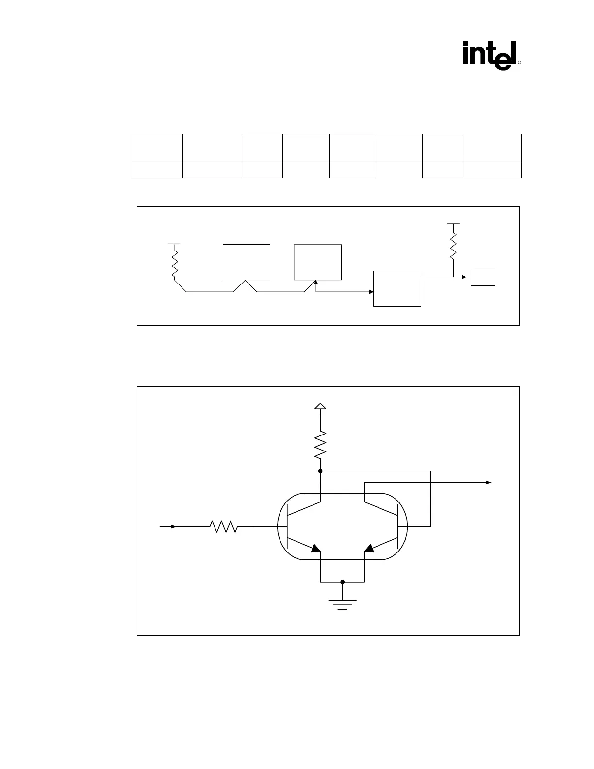
Level shifting is required for the INIT# signal to the FWH in order to meet the input logic levels of
the FWH. Figure 38 illustrates one method of implementing this level shifting.
Figure 38. Voltage Translation of INIT#
4.7k
INIT# from
ICH2
4.7k
12V
I
N
I
T
#
@
F
W
H
Volt_Trans_INIT
 Loading...

