Memory Interface Routing
R
98 Intel
®
Pentium
®
4 Processor / Intel
®
850 Chipset Family Platform Design Guide
6.1.2.4 Signal Layer Alternation for Rambus RIMM Connector Pin
Compensation
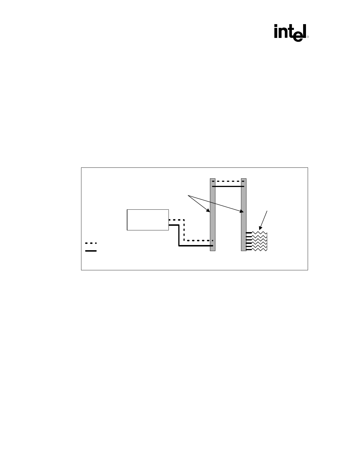
RSL and clocking signals must alternate layers as they are routed through the channel to
compensate for signals on bottom layer having to travel a longer distance through the pin
connector. This is illustrated in Figure 61. For example if a signal is routed on the top layer from
the MCH to the first RIMM connector, it must be routed on the bottom layer from the first RIMM
connector to the second RIMM connector. This rule also holds true for inner layer routing. If a
signal is routed on the top inner layer from the MCH to the first RIMM connector, it must be
routed on the bottom inner layer from the first RIMM connector to the second RIMM connector.
All RSL and clocking signals from the second RIMM connector to the termination resistor should
be routed on the top layer.
Figure 61. RSL and Clocking Signal Layer Alteration
RSL-CLK_Lay_Alt
Termination
RIMM
Connector
MCH
Signal on Layer X
Signal on Layer Y
Signal A
Signal B
Signal A
Signal B
On either layer,
ground isolation
is REQUIRED
6.1.2.5 Rambus RIMM Connector Impedance Compensation
The RIMM connector inductance has been shown to cause an impedance discontinuity on the
Direct Rambus channel. This can reduce voltage and timing margin. In order to compensate for the
inductance of the connector, a compensating capacitance is required on each RSL and clocking
connector pin. This compensating capacitance must be added to the following connector pins at
each connector
• LCTM
• LCTM#
• RCTM
• RCTM#
• CMD
• LCFM
• LCFM#
• RCFM
• RCFM#
• SCK
• LROW[2:0]
• RROW[2:0]
• LCOL[4:0]
• RCOL[4:0]
• RDQA[8:0]
• LDQA[8:0]
• RDQB[8:0]
• LDQB[8:0]
 Loading...

