Memory Interface Routing
R
104 Intel
®
Pentium
®
4 Processor / Intel
®
850 Chipset Family Platform Design Guide
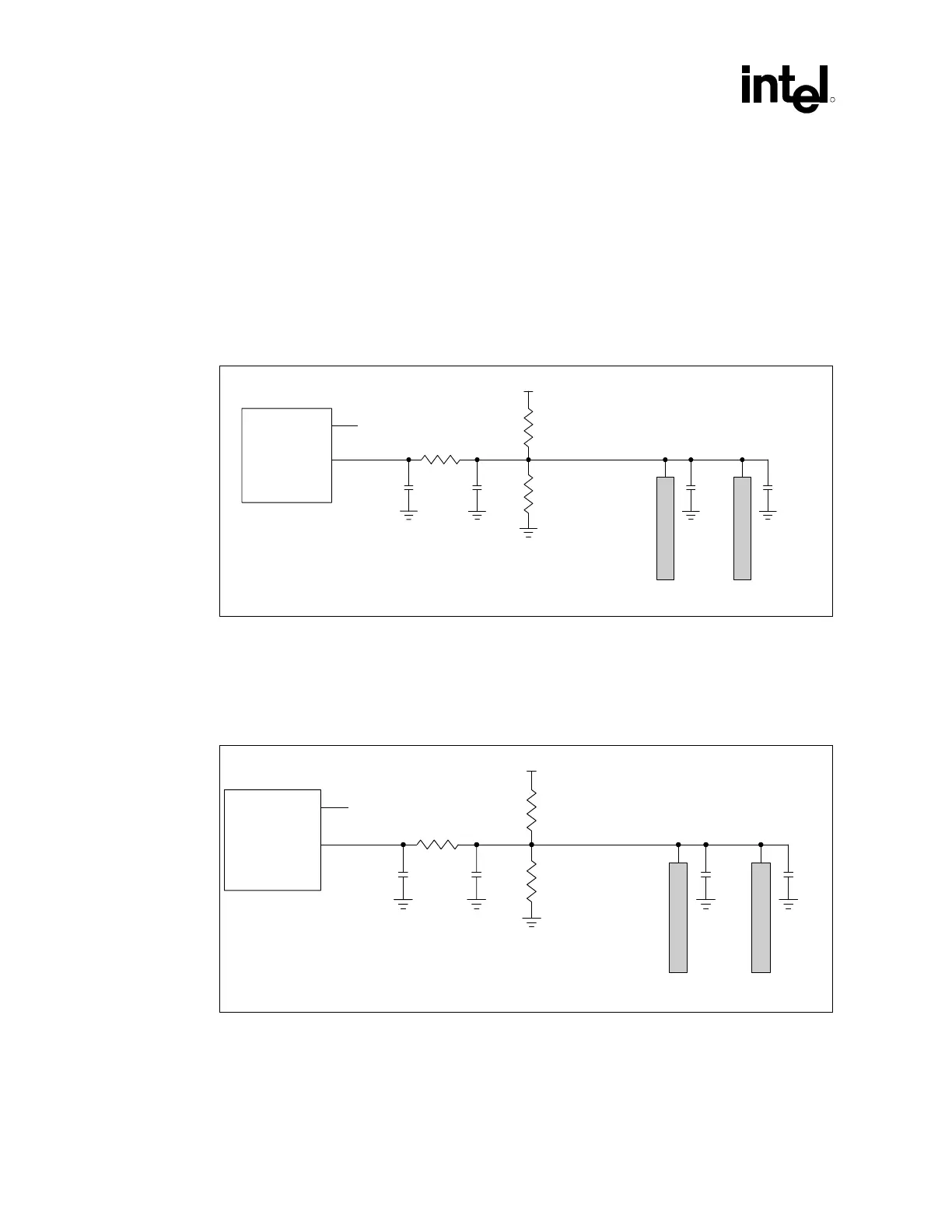
6.1.4 Rambus RDRAM* Device Reference Voltage
The RDRAM device reference voltage (RAMREF) must be generated as shown in Figure 67 for
300/400 MHz RDRAM technology designs and Figure 68 for 533 MHz RDRAM technology
designs. RAMREF should be generated from a typical resistor divider using 2% tolerant resistors.
Additionally, RAMREF must be decoupled locally at each RIMM connector, at the resistor divider
network, and at the MCH. Finally, a 100 Ω series resistor is required near the MCH. The
RAMREF signal should be routed with 10 mils wide traces.
Figure 67. RAMREF Generation Example Circuit for 300/400 MHz Rambus RDRAM*
Technology
CHA_REF[1:0]
CHB_REF[1:0]
0.1 uF
100
Ω
75 Ω (2%)
Vterm
MCH
0.1 uF
300 Ω (2%)
R
I
M
M
R
I
M
M
0.1 uF 0.1 uF
ramref_gen_circuit
Same as CHB_REF[1:0]
NOTE: The RAMREF Generation Circuit is not shown for Channel A in Figure 67, but is the same as the one
shown for Channel B.
Figure 68. RAMREF Generation Example Circuit for 533 MHz Rambus RDRAM* Technology
CHA_REF[1:0]
CHB_REF[1:0]
0.1 uF
100 Ω
84.5 Ω (1%)
Vterm
MCH
0.1 uF
255 Ω (1%)
R
I
M
M
R
I
M
M
0.1 uF 0.1 uF
ramref_gen_circuit_1066
Same as CHB_REF[1:0]
NOTE: The RAMREF Generation Circuit is not shown for Channel A in Figure 68, but is the same as the one
shown for Channel B.
 Loading...

