Schematic Review Checklist
R
252 Intel
®
Pentium
®
4 Processor / Intel
®
850 Chipset Family Platform Design Guide
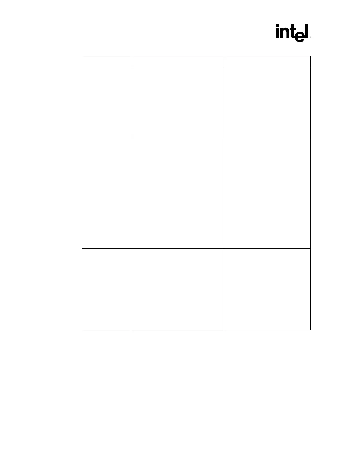
Checklist Items Recommendations Reason/Impact
I/O Decoupling
requirements
• 4 minimum, 5 preferred 0.1 µf
capacitors with 603 packages
distributed evenly over the System Bus
data lines.
• 2 minimum, 3 preferred 0.1 µf
capacitors with 603 packages
distributed evenly over the system bus
address and control lines.
• All capacitors placed as close as
possible to the MCH package (within
150 mils)
• This is to provide clean power
delivery to the system bus I/O ring.
• Refer to Section 5.5.1.
1.8 V RAC Power
Isolation
• Option 1 — Low pass filter with
inductor:
Place 3.3 nH inductor
between V
CC
RAC and the 1.8 V power
plane. Place a 3.3 µf capacitor on MCH
side of the inductor. Place 2–3 0.1 µF
capacitors near the V
CC
RAC pins for
adequate decoupling between V
CC
RAC
and VSS. Use 0805 size components.
• Option 1 — Low pass filter with
Ferrite Bead:
Place 10 Ω ( at
100 MHz) between V
CC
RAC and the
1.8 V power plane. Place a 10 µF
capacitor on MCH side of the inductor.
Use a minimum of 2 .1 µF capacitors
per RAC and a minimum of one 1.0 µF
capacitor for both RACs located near
the V
CC
RAC pins. Use 0805 size
components except for the 10 µF
capacitor, which can be 1206.
• The Intel 850/850E chipset requires
a low-pass filter on the V
CC
RAC
pins to meet clock jitter
specifications. The low-pass filter
isolates V
CC
RAC from the 1.8
voltage plane that powers the MCH
core.
• Refer to Section 12.3.
SCK/CMD Circuitry • This implementation is applicable for
RIMM* modules down solution only.
Also, this implementation is not
necessary if Suspend-to-RAM is not
supported in the system.
• Transistor needs to be connected to
SCK and should be gated with
PWROK circuitry. A dummy transistor
needs to be connected to the CMD
signal to minimize impedance
discontinuities.
• The transistor should have a Cobo of
4 pF or less.
• This circuitry is needed to avoid the
MCH inadvertently taking the
RDRAM devices out of power-down
due to the CMOS interface being
driven during power ramp, the SCK
signal should be shunted to ground
when the MCH is entering and
exiting Suspend-to-RAM.
• Refer to Section 6.1.7.
 Loading...

