R8C/20 Group, R8C/21 Group 1. Overview
Rev.2.00 Aug 27, 2008 Page 2 of 458
REJ09B0250-0200
1.2 Performance Overview
Table 1.1 outlines the Functions and Specifications for R8C/20 Group and Table 1.2 outlines the Functions and
Specifications for R8C/21 Group.
NOTES:
1. When using options, be sure to inquire about the specification.
2. I
2
C bus is a registered trademark of Koninklijke Philips Electronics N.V.
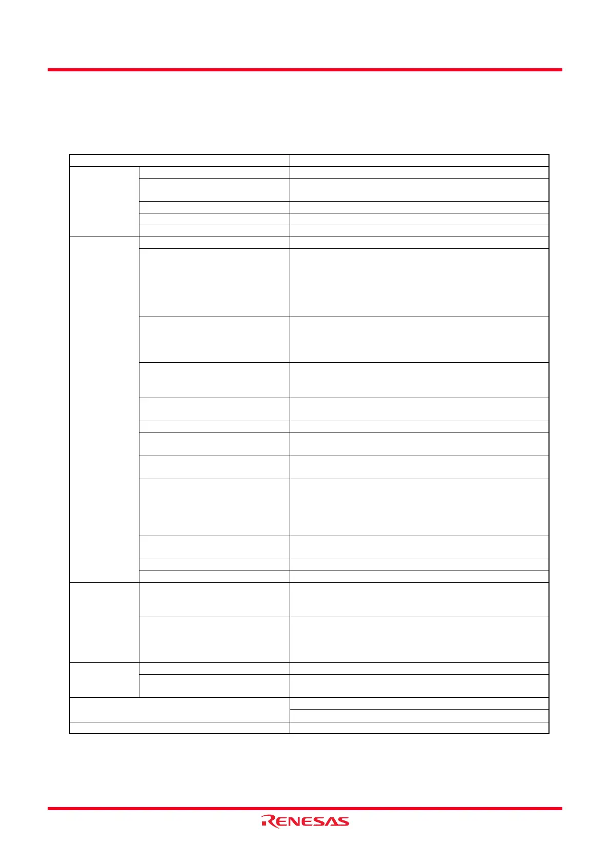
Table 1.1 Functions and Specifications for R8C/20 Group
Item Specification
CPU Number of fundamental instructions 89 instructions
Minimum instruction execution time 50 ns (f(XIN) = 20 MHz, VCC = 3.0 to 5.5 V)
100 ns (f(XIN) = 10 MHz, VCC = 2.7 to 5.5 V)
Operating mode Single-chip
Address space 1 Mbyte
Memory capacity Refer to Table 1.3 Product Information for R8C/20 Group
Peripheral
Function
Ports I/O ports: 41 pins, Input port: 3 pins
Timers Timer RA: 8 bits x 1 channel,
Timer RB: 8 bits x 1 channel
(Each timer equipped with 8-bit prescaler)
Timer RD: 16 bits x 2 channel
(Circuits of input capture and output compare)
Timer RE: With compare match function
Serial interface 1 channel (UART0)
Clock synchronous I/O, UART
1 channel (UART1)
UART
Clock synchronous serial interface
1 channel
I
2
C bus interface
(2)
, Clock synchronous serial I/O with chip
select
LIN module
Hardware LIN: 1 channel
(timer RA, UART0)
A/D converter 10-bit A/D converter: 1 circuit, 12 channels
Watchdog timer 15 bits x 1 channel (with prescaler)
Reset start selectable
Interrupt Internal: 11 sources, External: 5 sources, Software: 4 sources,
Priority level: 7 levels
Clock generation circuits 2 circuits
XIN clock generation circuit (with on-chip feedback resistor)
On-chip oscillator (high speed, low speed)
High-speed on-chip oscillator has frequency adjustment
function.
Oscillation stop detection
function
Stop detection of XIN clock oscillation
Voltage detection circuit On-chip
Power-on reset circuit include On-chip
Electric
Characteristics
Supply voltage VCC = 3.0 to 5.5 V (f(XIN) = 20 MHz)(J version)
VCC = 3.0 to 5.5 V (f(XIN) = 16 MHz)(K version)
VCC = 2.7 to 5.5 V (f(XIN) = 10 MHz)
Current consumption Typ. 11.0 mA (VCC = 5 V, f(XIN) = 20 MHz, High-speed on-
chip oscillator stopping)
Typ. 5.3 mA (VCC = 5 V, f(XIN) = 10 MHz, High-speed on-chip
oscillator stopping)
Flash Memory Programming and erasure voltage VCC = 2.7 to 5.5 V
Programming and erasure
endurance
100 times
Operating Ambient Temperature -40 to 85°C
-40 to 125°C (option
(1)
)
Package 48-pin mold-plastic LQFP
 Loading...