R8C/20 Group, R8C/21 Group 1. Overview
Rev.2.00 Aug 27, 2008 Page 8 of 458
REJ09B0250-0200
1.6 Pin Functions
Table 1.5 lists the Pin Functions and Table 1.6 lists the Pin Name Information by Pin Number.
I: Input O: Output I/O: Input and output
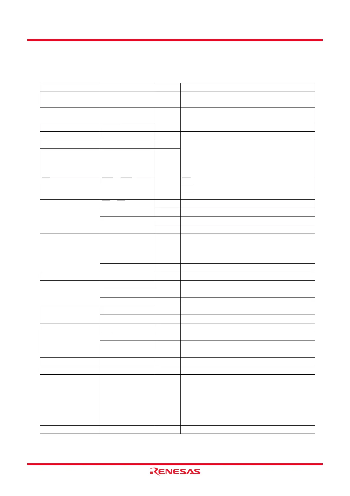
Table 1.5 Pin Functions
Type Symbol I/O Type Description
Power Supply Input VCC
VSS
I Apply 2.7 V to 5.5 V to the VCC pin. Apply 0 V to the
VSS pin.
Analog Power Supply
Input
AVCC, AVSS I Applies the power supply for the A/D converter. Connect
a capacitor between AVCC and AVSS.
Reset Input RESET
I Input “L” on this pin resets the MCU.
MODE MODE I Connect this pin to VCC via a resistor.
XIN Clock Input XIN I These pins are provided for the XIN clock generation
circuit I/O. Connect a ceramic resonator or a crystal
oscillator between the XIN and XOUT pins. To use an
externally derived clock, input it to the XIN pin and leave
the XOUT pin open.
XIN Clock Output XOUT O
INT
Interrupt Input INT0 to INT3 IINT interrupt input pins.
INT0
Timer RD input pins.
INT1
Timer RA input pins.
Key Input Interrupt KI0
to KI3 I Key input interrupt input pins.
Timer RA TRAIO I/O Timer RA I/O pin.
TRAO O Timer RA output pin.
Timer RB TRBO O Timer RB output pin.
Timer RD TRDIOA0, TRDIOA1,
TRDIOB0, TRDIOB1,
TRDIOC0, TRDIOC1,
TRDIOD0, TRDIOD1
I/O Timer RD I/O ports.
TRDCLK I External clock input pin.
Timer RE TREO O Divided clock output pin.
Serial Interface CLK0 I/O Transfer clock I/O pin.
RXD0, RXD1 I Serial data input pins.
TXD0, TXD1 O Serial data output pins.
I
2
C Bus Interface
SCL I/O Clock I/O pin.
SDA I/O Data I/O pin.
Clock Synchronous
Serial I/O with Chip
Select
SSI I/O Data I/O pin.
SCS
I/O Chip-select signal I/O pin.
SSCK I/O Clock I/O pin.
SSO I/O Data I/O pin.
Reference Voltage Input VREF I Reference voltage input pin to A/D converter.
A/D Converter AN0 to AN11 I Analog input pins to A/D converter.
I/O Port P0_0 to P0_7,
P1_0 to P1_7,
P2_0 to P2_7,
P3_0, P3_1,
P3_3 to P3_5, P3_7,
P4_3 to P4_5,
P6_0 to P6_7
I/O CMOS I/O ports. Each port contains an input/output
select direction register, allowing each pin in that port to
be directed for input or output individually.
Any port set to input can select whether to use a pull-up
resistor or not by a program.
Input Port P4_2, P4_6, P4_7 I Input only ports.
 Loading...