R8C/20 Group, R8C/21 Group 14. Timers
Rev.2.00 Aug 27, 2008 Page 165 of 458
REJ09B0250-0200
14.3.2 Buffer Operation
The TRDGRCi register can be used as the buffer register of the TRDGRAi register, and the TRDGRDi register
can be used as the buffer register of the TRDGRBi register by the BFCi and BFDi bits in the TRDMR register.
• TRDGRAi buffer register: TRDGRCi register
• TRDGRBi buffer register: TRDGRDi register
Buffer operation depends on modes. Table 14.22 lists the Buffer Operation in Each Mode.
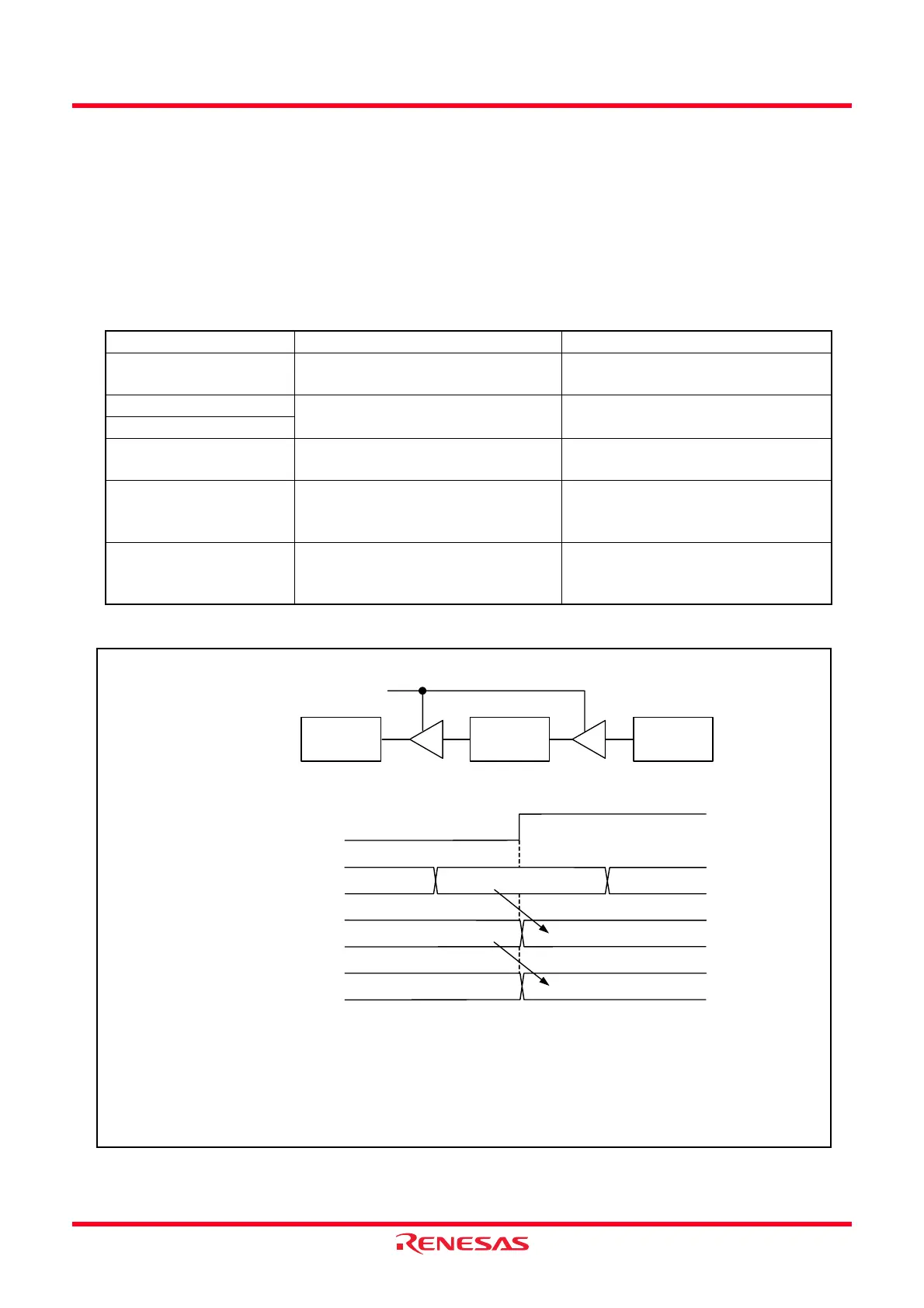
Figure 14.29 shows the Buffer Operation in Input Capture Function, and Figure 14.30 shows the Buffer
Operation in Output Compare Function.
i = 0 or 1
Figure 14.29 Buffer Operation in Input Capture Function
Table 14.22 Buffer Operation in Each Mode
Function and Mode Transfer Timing Transfer Register
Input Capture Function Input capture signal input Transfer content in TRDGRAi
(TRDGRBi) register to buffer register
Output Compare Function Compare match with TRDi register
and TRDGRAi (TRDGRBi) register
Transfer content in buffer register to
TRDGRAi (TRDGRBi) register
PWM Mode
Reset Synchronous PWM
Mode
Compare match withTRD0 register
and TRDGRA0 register
Transfer content in buffer register to
TRDGRAi (TRDGRBi) register
Complementary PWM
Mode
• Compare match with TRD0 register
and TRDGRA0 register
• TRD1 register underflow
Transfer content in buffer register to
TRDGRB0, TRDGRA1 and
TRDGRB1 registers
PWM3 Mode Compare match with TRD0 register
and TRDGRA0 register
Transfer content in buffer register to
TRDGRA0, TRDGRB0, TRDGRA1
and TRDGRB1 registers
m
Transfer
n
TRDGRAi register
n-1
n+1
TRDIOAi input
TRDi register
i = 0 or 1
The above applies to the following conditions:
• The BFCi bit in the TRDMR register is set to 1. (The TRDGRCi register is used as the buffer register of
the TRDGRAi register.)
• The IOA2 to IOA0 bits in the TRDIORAi register are set to 100b (input capture at the falling edge).
m
Transfer
TRDGRCi register
(buffer)
n
TRDGRCi
register
(buffer)
TRDGRAi
register
TRDi
TRDIOAi input
(input capture signal)
 Loading...