R8C/20 Group, R8C/21 Group 14. Timers
Rev.2.00 Aug 27, 2008 Page 164 of 458
REJ09B0250-0200
14.3.1 Count Source
The count source selection can be used in all modes. However, in PWM3 mode, the external clock cannot be
selected.
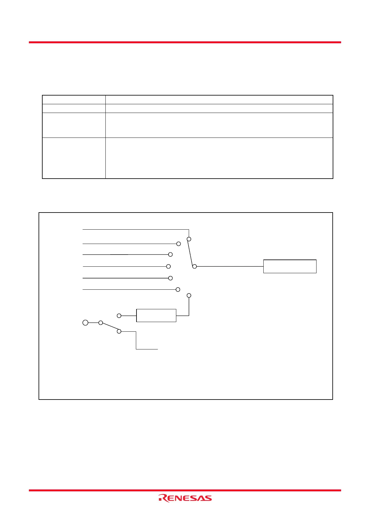
i = 0 or 1
NOTE:
1. The count source fOCO40M can be used with VCC = 3.0 to 5.5 V.
Figure 14.28 Block Diagram of Count Source
Set the pulse width of the external clock which inputs to the TRDCLK pin to 3 cycles or above of the operation
clock of Timer RD (refer to Table 14.11 Timer RD Operation Clocks).
When selecting fOCO40M for the count source, set the FRA00 bit in the FRA0 register to 1 (high-speed on-
chip oscillator on) before setting the TCK2 to TCK0 bits in the TRDCRi register (i = 0 or 1) to 110b
(fOCO40M).
Table 14.21 Count Source Selection
Count Source Selection
f1, f2, f4, f8, f32 The count source is selected by bits TCK2 to TCK0 in the TRDCRi register.
fOCO40M
(1)
The FRA00 bit in the FRA0 register is set to 1 (high-speed on-chip oscillator
frequency).
Bits TCK2 to TCK0 in the TRDCRi register is set to 110b (fOCO40M).
External Signal Input
to TRDCLK Pin
The STCLK bit in the TRDFCR register is set to 1 (external clock input enabled).
The TCK2 to TCK0 bits in the TRDCRi register are set to 101b
(count source: external clock).
The valid edge selected by the CKEG1 to CKEG0 bits in the TRDCRi register.
The PD2_0 bit in the PD2 register is set to 0 (input mode).
TRDCLK/
TRDIOA0
TCK2 to TCK0
TRDi register
i = 0 or 1
TCK2 to TCK0, CKEG1 to CKEG0: Bits in TRDCRi register
STCLK: Bit in TRDFCR register
f1
f2
f4
f8
f32
= 001b
= 010b
= 011b
= 000b
= 101b
= 100b
Valid edge
selected
CKEG1 to CKEG0
TRDIOA0 I/O or programmable I/O port
Count source
STCLK = 1
STCLK = 0
fOCO40M
= 110b
 Loading...