R8C/20 Group, R8C/21 Group 19. Flash Memory
Rev.2.00 Aug 27, 2008 Page 381 of 458
REJ09B0250-0200
19.3.2 ROM Code Protect Function
The ROM code protect function disables to read and change the internal flash memory by the OFS register in
parallel I/O mode.
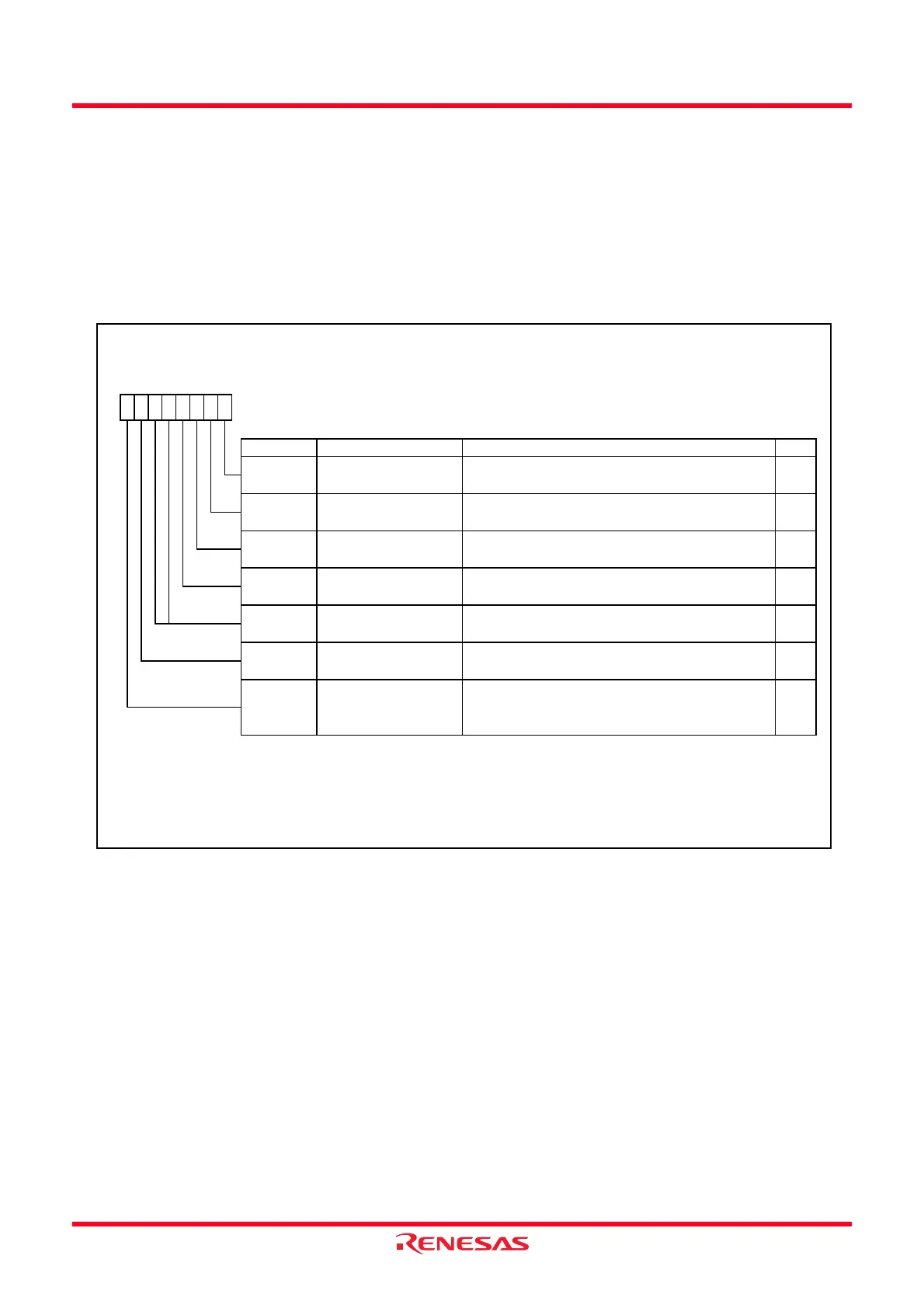
Figure 19.4 shows the OFS Register.
The ROM code protect function is enabled by writing 0 to the ROMCP1 bit and 1 to the ROMCR bit and
disables to read and change the internal flash memory.
Once the ROM code protect is enabled, the content in the internal flash memory cannot be rewritten in parallel
I/O mode. When the ROM code protect is disabled, erase the block including the OFS register with CPU
rewrite mode or standard serial I/O mode.
Figure 19.4 OFS Register
Option Function Select Register
(1)
Symbol Address Before Shipment
OFS
0FFFFh FFh
(3)
Bit Symbol Bit Name Function RW
Reserved bit
NOTES:
1.
2.
3.
b7 b6 b5 b4 b3 b2 b1 b0
11 1
—
(b1)
Set to 1
RW
WDTON
Watchdog timer start
select bit
0 : Starts w atchdog timer automatically after reset
1 : Watchdog timer is inactive after reset
RW
ROMCR
ROM code protect
disabled bit
0 : ROM code protect disabled
1 : ROMCP1 enabled
RW
ROMCP1
ROM code protect bit 0 : ROM code protect enabled
1 : ROM code protect disabled
RW
RW
—
(b5-b4)
Reserved bits Set to 1
RW
If the block including the OFS register is erased, FFh is set to the OFS register.
To use the pow er-on reset, set the LVD1ON bit to 0 (voltage monitor 1 reset enabled after reset).
LVD1ON
Voltage detection circuit
start bit
(2)
0 : Voltage monitor 1 reset enabled after reset
1 : Voltage monitor 1 reset disabled after reset
RW
The OFS register is on the flash memory. Write to the OFS register w ith a program. After w riting is completed, do not
w rite additions to the OFS register.
CSPROINI
Count source protect
mode after reset select
bit
0 : Count source protect mode enabled after reset
1 : Count source protect mode disabled after reset