R8C/20 Group, R8C/21 Group 14. Timers
Rev.2.00 Aug 27, 2008 Page 237 of 458
REJ09B0250-0200
14.3.10 PWM3 Mode
Output 2 PWM waveforms with the same period.
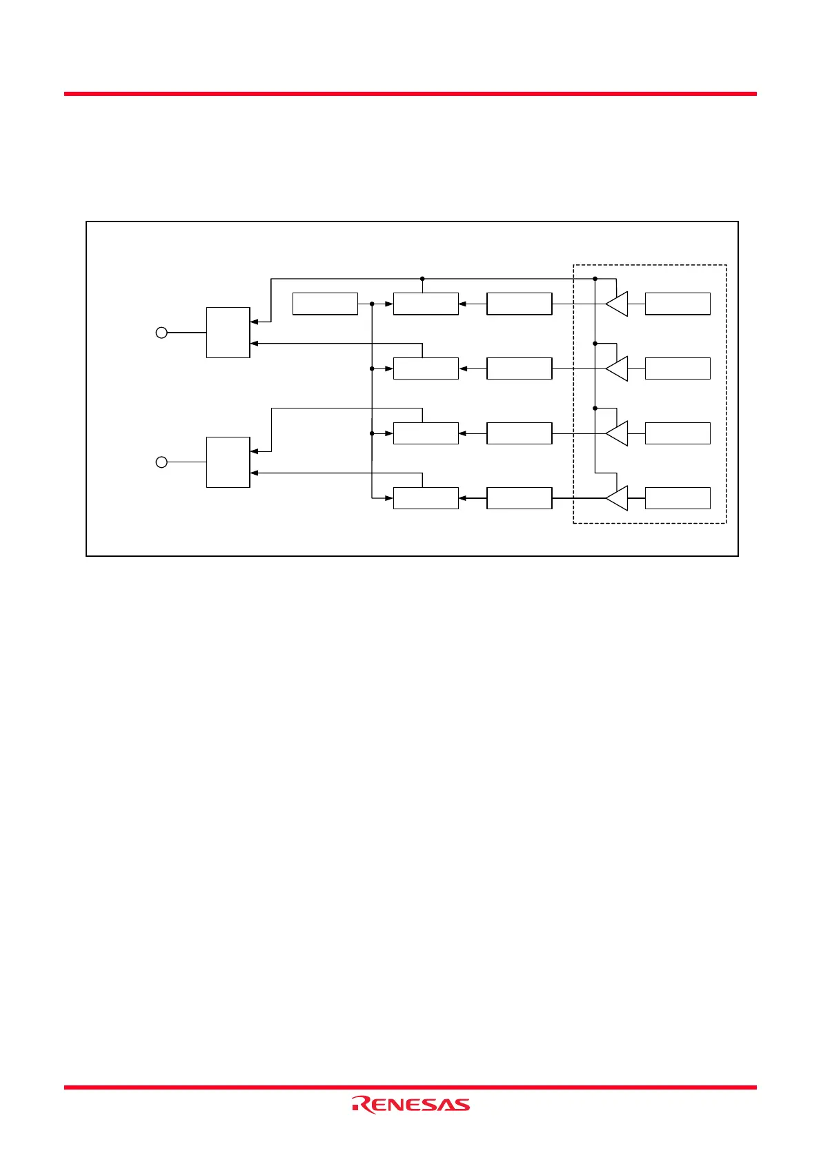
Figure 14.98 shows the Block Diagram of PWM3 Mode, Table 14.33 lists the PWM3 Mode Specifications.
Figures 14.99 to 14.107 show the Registers Associated with PWM3 Mode and Figure 14.108 shows the
Operating Example of PWM3 Mode.
Figure 14.98 Block Diagram of PWM3 Mode
TRDIOA0
Output
control
TRDGRC0
Compare match signal
TRDIOB0
Output
control
Comparator TRDGRA0TRD0
TRDGRC1
Compare match signal
Comparator TRDGRA1
TRDGRD0Comparator TRDGRB0
TRDGRD1Comparator TRDGRB1
Compare match signal
Compare match signal
Buffer
 Loading...