R8C/20 Group, R8C/21 Group 15. Serial Interface
Rev.2.00 Aug 27, 2008 Page 274 of 458
REJ09B0250-0200
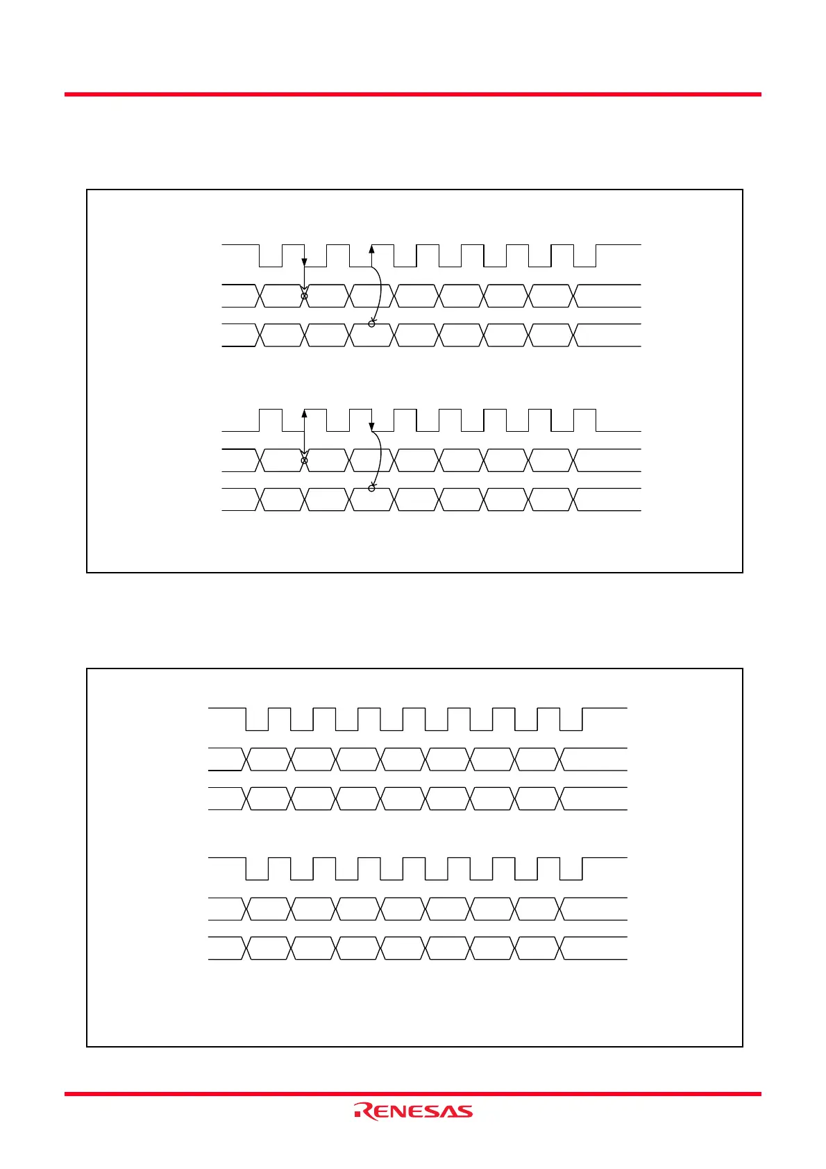
15.1.1 Polarity Select Function
Figure 15.8 shows the Transfer Clock Polarity. Use the CKPOL bit in the U0C0 register to select the transfer
clock polarity.
Figure 15.8 Transfer Clock Polarity
15.1.2 LSB First/MSB First Select Function
Figure 15.9 shows the Transfer Format. Use the UFORM bit in the U0C0 register to select the transfer format.
Figure 15.9 Transfer Format
CLK0
(1)
D0TXD0
• When the CKPOL Bit in the U0C0 Register = 0 (output transmit data at the falling
edge and input the receive data at the rising edge of the transfer clock)
D1 D2
NOTES:
1. When not transferring, the CLK0 pin level is “H”.
2. When not transferring, the CLK0 pin level is “L”.
D3 D4 D5 D6 D7
D0RXD0 D1 D2 D3 D4 D5 D6 D7
CLK0
(2)
D0TXD0 D1 D2 D3 D4 D5 D6 D7
D0RXD0 D1 D2 D3 D4 D5 D6 D7
• When the CKPOL Bit in the U0C0 Register = 1 (output transmit data at the rising
edge and input the receive data at the falling edge of the transfer clock)
CLK0
D0TXD0
• When UFORM Bit in U0C0 Register = 0 (LSB first)
(1)
D1 D2 D3 D4 D5 D6 D7
D0RXD0 D1 D2 D3 D4 D5 D6 D7
CLK0
D7
TXD0 D6 D5 D4 D3 D2 D1 D0
RXD0
• When UFORM Bit in U0C0 Register = 1 (MSB first)
(1)
NOTE:
1. The above applies when the CKPOL bit in the U0C0 register is set to 0
(output transmit data at the falling edge and input receive data at the
rising edge of the transfer clock).
D7 D6 D5 D4 D3 D2 D1 D0
 Loading...