R8C/20 Group, R8C/21 Group 1. Overview
Rev.2.00 Aug 27, 2008 Page 4 of 458
REJ09B0250-0200
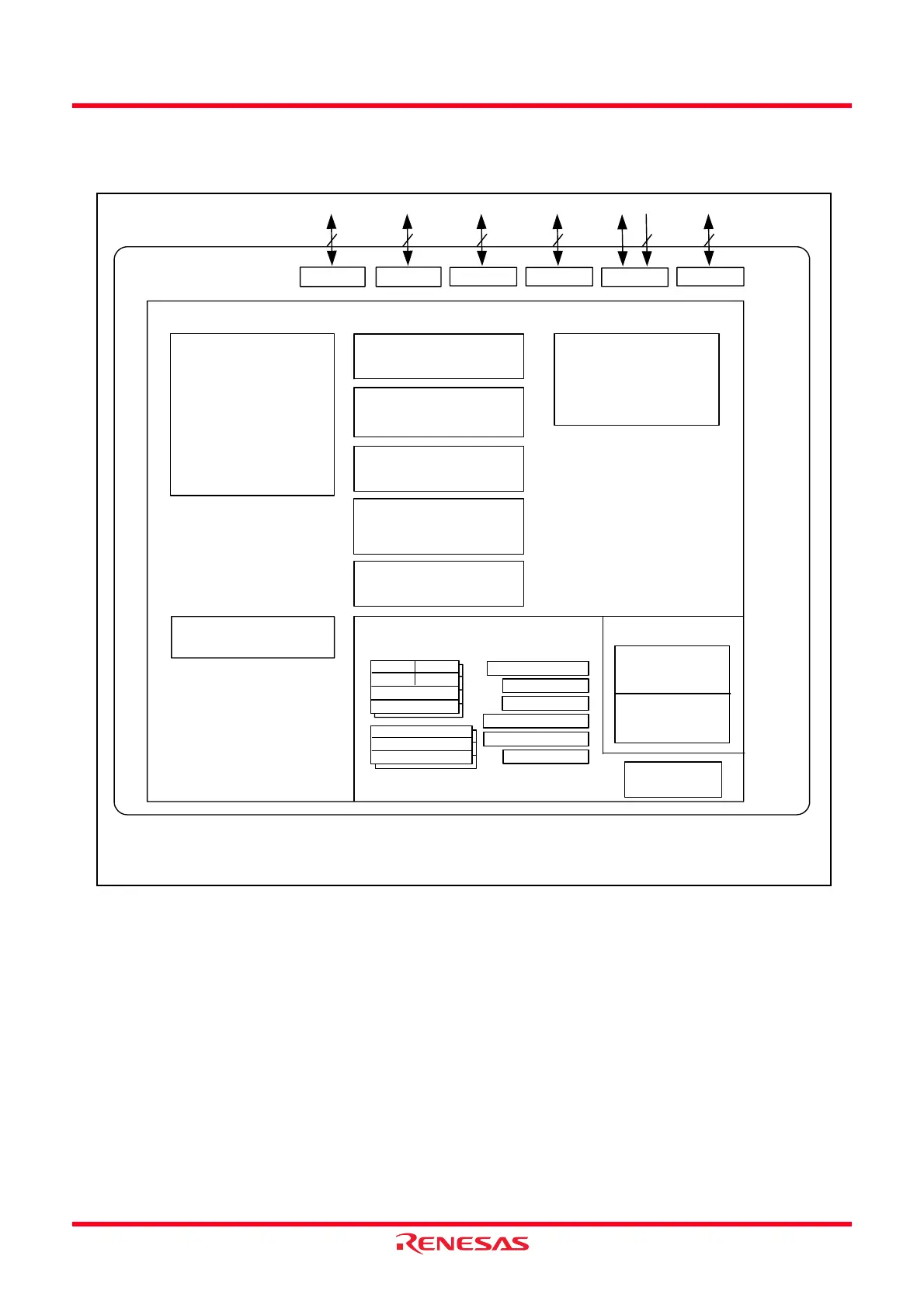
1.3 Block Diagram
Figure 1.1 shows a Block Diagram.
Figure 1.1 Block Diagram
R8C CPU core
Timer
Timer RA (8 bits)
Timer RB (8 bits)
Timer RD (16 bits
× 2 channels)
Timer RE (8 bits)
A/D converter
(10 bits
× 12 channels)
System clock
generation circuit
XIN-XOUT
High-speed on-chip oscillator
Low-speed on-chip oscillator
UART or
clock synchronous serial I/O
(8 bits × 1 channel)
Memory
Watchdog timer
(15 bits)
ROM
(1)
RAM
(2)
Multiplier
R0H R0L
R1H
R2
R3
R1L
A0
A1
FB
SB
USP
ISP
INTB
PC
FLG
I/O port
NOTES:
1. ROM size depends on MCU type.
2. RAM size depends on MCU type.
I
2
C bus interface or
clock synchronous serial I/O
with chip select
(8 bits × 1 channel)
8
Port P1
6
Port P3
3 3
Port P4
8
Port P0
8
Port P2
8
Port P6
UART
(8 bits
× 1 channel)
LIN module
(1 channel)
 Loading...