R8C/20 Group, R8C/21 Group 14. Timers
Rev.2.00 Aug 27, 2008 Page 166 of 458
REJ09B0250-0200
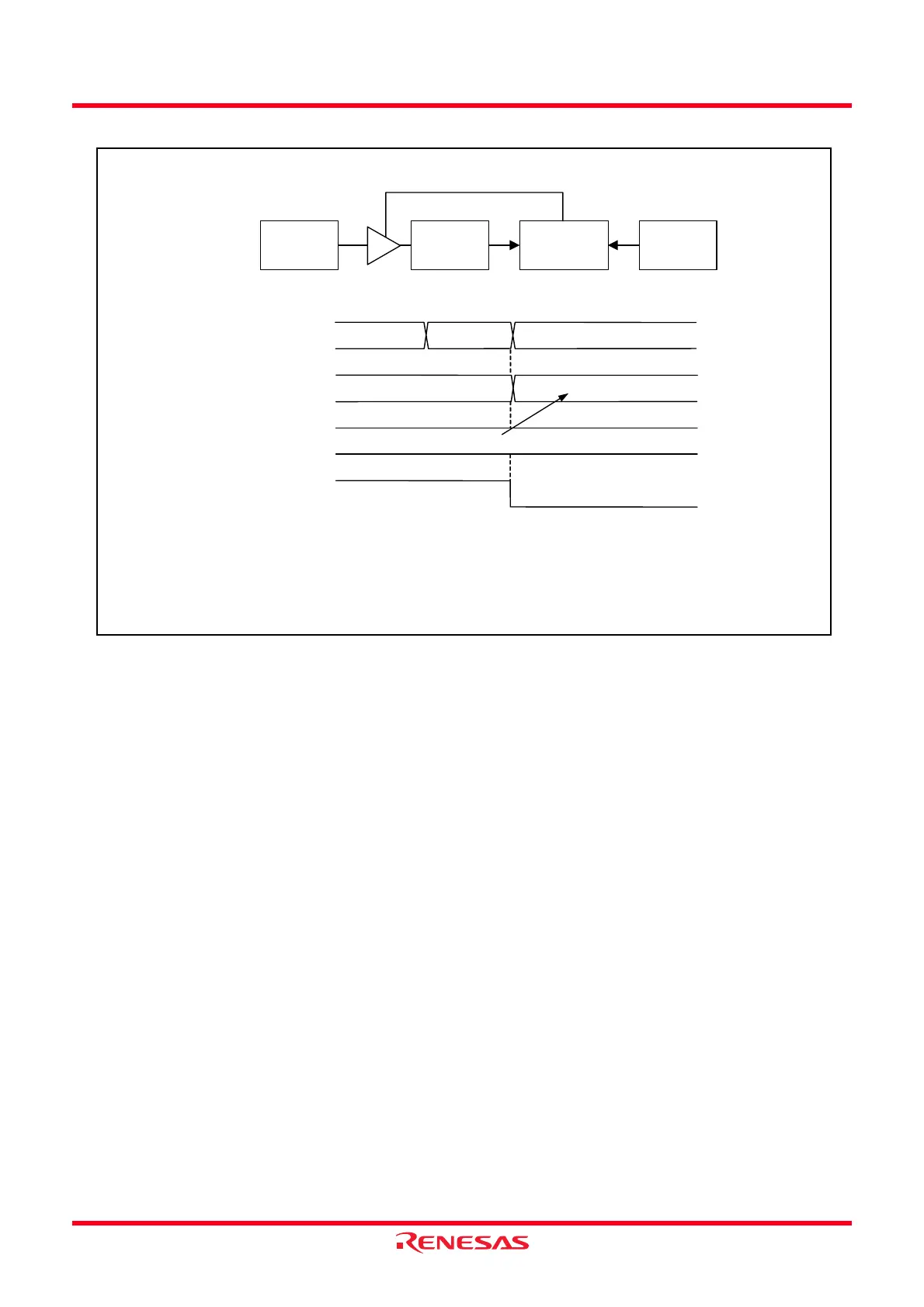
Figure 14.30 Buffer Operation in Output Compare Function
Perform the following for the timer mode (input capture and output compare functions).
When using the TRDGRCi (i = 0 or 1) register as the buffer register of the TRDGRAi register
• Set the IOC3 bit in the TRDIORCi register to 1 (general register or buffer register).
• Set the IOC2 bit in the TRDIORCi register to the same as the IOA2 bit in the TRDIORAi register.
When using the TRDGRDi register as the buffer register of the TRDGRBi register
• Set the IOD3 bit in the TRDIORDi register to 1 (general register or buffer register).
• Set the IOD2 bit in the TRDIORCi register to the same value as the IOB2 bit in the TRDIORAi register.
Bits IMFC and IMFD in the TRDSRi register are set to 1 at the input edge of the TRDIOCi pin when also using
registers TRDGRCi and TRDGRDi as the buffer register in the input capture function.
When using the TRDGRCi and TRDGRDi registers for the buffer register in output compare function, reset
synchronous PWM mode, complementary PWM mode and PWM3 mode, the IMFC and IMFD bits in the
TRDSRi register are set to 1 by the compare match with the TRDi register.
mnTRDGRAi register
m-1
m+1
TRDi register
i = 0 or 1
The above applies to the following conditions:
• BFCi bit in the TRDMR register is set to 1. (The TRDGRCi register is used as the buffer register of
the TRDGRAi register.)
• IOA2 to IOA0 bits in the TRDIORAi register are set to 001b (“L” output by the compare match).
n
Transfer
TRDGRCi register
(buffer)
m
TRDIOAi output
TRDGRCi
register
(buffer)
TRDGRAi
register
Comparator TRDi
Compare match signal
 Loading...