R8C/20 Group, R8C/21 Group 14. Timers
Rev.2.00 Aug 27, 2008 Page 219 of 458
REJ09B0250-0200
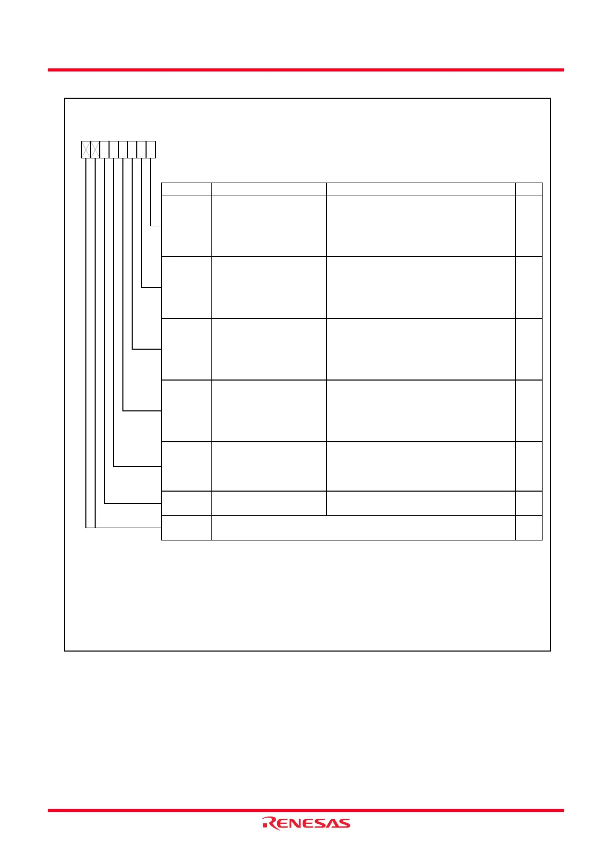
Figure 14.81 Registers TRDSR0 to TRDSR1 in Reset Synchronous PWM Mode
Timer RD Status Register i (i = 0 or 1)
Symbol Address After Reset
TRDSR0
TRDSR1
0143h
0153h
11100000b
11000000b
Bit Symbol Bit Name Function RW
NOTES:
1.
2.
3.
—
(b7 - b6)
—
Nothing is assigned. If necessary, set to 0.
When read, the content is 1.
RWOVF
UDF
Underflow flag
(1)
This bit is disabled in reset synchronous PWM
mode.
RW
Input capture/compare match
flag C
[Source for setting this bit to 0]
Write 0 after read.
(2)
[Source for setting this bit to 1]
When the value in the TRDi register matches w ith
the value in the TRDGRCi register.
(3)
Nothing is assigned to the b5 in the TRDSR0 register. When w riting to the b5, w rite 0. When reading, its content is 1.
IMFC RW
RW
Input capture/compare match
flag D
[Source for setting this bit to 0]
Write 0 after read.
(2)
[Source for setting this bit to 1]
When the value in the TRDi register matches w ith
the value in the TRDGRDi register.
(3)
Overflow flag [Source for setting this bit to 0]
Write 0 after read.
(2)
[Source for setting this bit to 1]
When the TRDi register overflows.
RW
IMFB RW
Input capture/compare match
flag A
[Source for setting this bit to 0]
Write 0 after read.
(2)
[Source for setting this bit to 1]
When the value in the TRDi register matches
w ith the value in the TRDGRAi register.
Input capture/compare match
flag B
[Source for setting this bit to 0]
Write 0 after read.
(2)
[Source for setting this bit to 1]
When the value in the TRDi register matches
w ith the value in the TRDGRBi register.
IMFA
b7 b6 b5 b4
Including w hen the BFji bit in the TRDMR register is set to 1 (TRDGRji is used as the buffer register).
The writing results are as follow s:
• This bit is set to 0 w hen the read result is 1 and w riting 0 to the same bit.
• This bit remains unchanged even if the read result is 0 and w riting 0 to the same bit. (This bit remains 1 even if this
bit is set to 1 from 0 after reading, and writing 0.)
• This bit remains unchanged w hen w riting 1.
b3 b2
IMFD
b1 b0

 Loading...