R8C/20 Group, R8C/21 Group 14. Timers
Rev.2.00 Aug 27, 2008 Page 225 of 458
REJ09B0250-0200
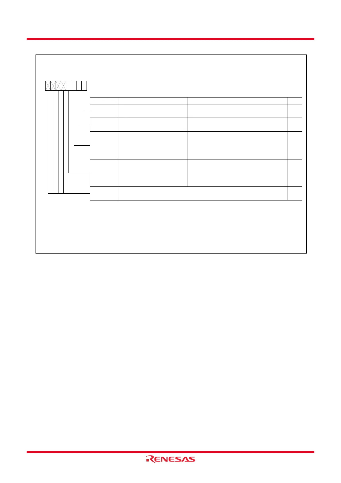
Figure 14.87 TRDSTR Register in Complementary PWM Mode
Timer RD Start Register
(1)
Symbol Address After Reset
TRDSTR
0137h 11111100b
Bit Symbol Bit Name Function RW
NOTES:
1.
2.
3.
4.
5.
When the CSEL0 bit is set to 1, w rite 0 to the TSTART0 bit.
When the CSEL1 bit is set to 1, w rite 0 to the TSTART1 bit.
When the CSEL0 bit is set to 0 and generating the compare match signal(TRDIOA0), this bit is set to 0 (count stops).
When the CSEL1 bit is set to 0 and generating the compare match signal(TRDIOA1), this bit is set to 0 (count stops).
Set the TRDSTR register using the MOV instruction (do not use the bit handling instruction). Refer to
14.3.12.1
TRDSTR Re gis te r
of
Notes on Timer RD.
TRD0 count operation select bit 0 : Count stops at the compare match
w ith the TRDGRA0 register
1 : Count continues at the compare
match w ith the TRDGRA0 register
CSEL0 RW
RW
TRD1 count operation select bit 0 : Count stops at the compare match
w ith the TRDGRA1 register
1 : Count continues at the compare
match w ith the TRDGRA1 register
—
—
(b7 - b4)
RW
TSTART1 RW
TRD1 count start flag
(5)
0 : Count stops
(3)
1 : Count starts
TRD0 count start flag
(4)
0 : Count stops
(2)
1 : Count starts
Nothing is assigned. If necessary, set to 0.
When read, the content is 1.
b7 b6 b5 b4 b3 b2
CSEL1
b1 b0
TSTART0
 Loading...