R8C/20 Group, R8C/21 Group 14. Timers
Rev.2.00 Aug 27, 2008 Page 235 of 458
REJ09B0250-0200
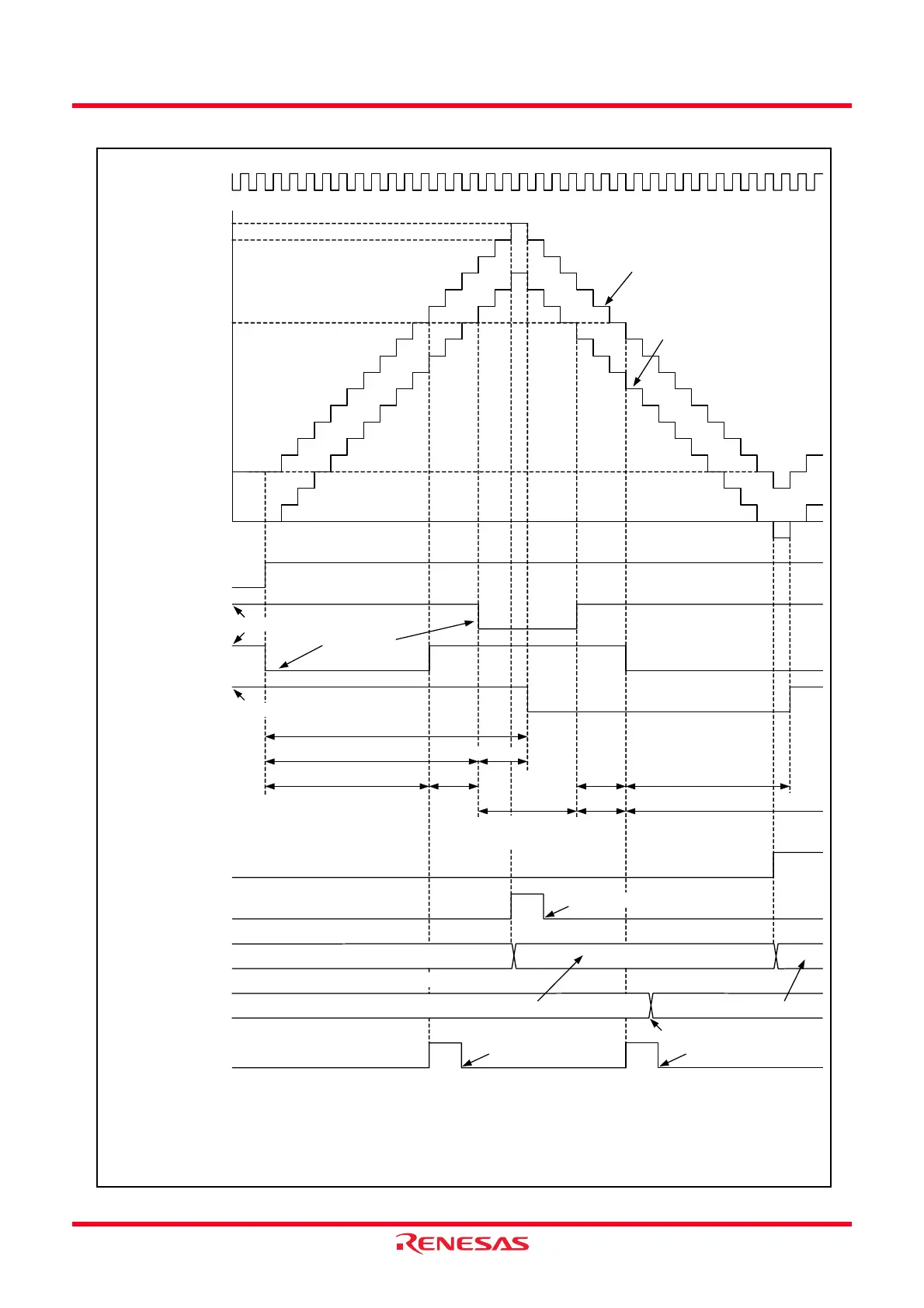
Figure 14.97 Operating Example of Complementary PWM Mode
m + 2 - p
p
n + 1
n + 1 - p p n + 1 - p
n
n
n
m - p - n + 1
m
n
Value in TRDi register
Count source
TRDIOD0 output
p
m: Setting Value in TRDGRA0 register
n: Setting Value in TRDGRB0 register
p: Setting Value in TRD0 register
TRDIOB0 output
IMFA bit in
TRDSR0 register
1
0
TRDGRB0 register
TSTART0 and TSTART1
bits in TRDSTR register
1
0
TRDIOC0 output
0000h
m + 1
(m - p - n + 1) × 2
Width of normal-
phase active level
Dead
time
(n + 1 - p) × 2
Width of counter-phase active level
Set to
FFFFh
1
0
UDF bit in
TRDSR1 register
1
0
Following data
Modify with a program
TRDGRD0 register
Transfer (When the CMD1 to CMD0 bits are set to 11b)
Transfer (When the CMD1 to CMD0 bits
are set to 10b)
Value in TRD1 register
Value in TRD0 register
CMD0, CMD1: Bits in TRDFCR register
i = 0 or 1
The above applies to the following conditions:
The OLS1 and OLS0 bits in the TRDFCR are set to 0 (initial output level “H”, active level “L” for normal-phase and counter-phase)
Set to 0 by a program
Active level “L”
Initial output “H”
Initial output “H”
Set to 0 by a program
Set to 0 by a program
IMFB bit in
TRDSR0 register
 Loading...