R8C/20 Group, R8C/21 Group 16. Clock Synchronous Serial Interface
Rev.2.00 Aug 27, 2008 Page 289 of 458
REJ09B0250-0200
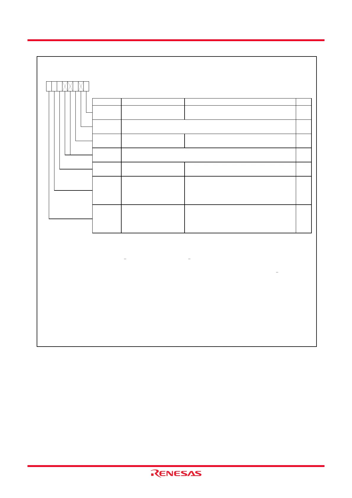
Figure 16.6 SSSR Register
SS Status Register
(7)
Symbol Address After Reset
SSSR
00BCh 00h
Bit Symbol Bit Name Function RW
NOTES:
1.
2.
3.
4.
5.
6.
7.
b0
When reading 1 and w riting 0, the CE, ORER, RDRF, TEND and TDRE bits are set to 0.
Indicates overrun error occurs and receive completes by error w hen receive. When the next serial data receive is
completed w hile the RDRF bit is set to 1 (data in the SSRDR register), the ORER bit is set to 1. After the ORER bit is
set to 1 (overrun error occurs), do not transmit or receive w hile the ORER bit is set to 1.
Nothing is assigned. If necessary, set to 0.
When read, the content is 0.
TDRE
Transmit data empty
(1,5,6)
0 : Data is not transferred from the SSTDR to
SSTRSR registers
1 : Data is transferred from the SSTDR to SSTRSR
registers
RW
b3 b2 b1b7 b6 b5 b4
RDRF
Receive data register full
(1,4)
—
(b1)
Nothing is assigned. If necessary, set to 0.
When read, the content is 0.
0 : No data in SSRDR register
1 : Data in SSRDR register
RW
ORER
—
(b4-b3)
CE RW
RW
—
Conflict error flag
(1)
0 : No conflict error occurs
1 : Conflict error occurs
(2)
—
The TDRE bit is set to 1 w hen settin
the TE bit in the SSER re
ister to 0
disables transmit
.
The RDRF bit is set to 0 w hen readin
out the data from the SSRDR re
ister.
Overrun error flag
(1)
0 : No overrun error occurs
1 : Overrun error occurs
(3)
The TEND and TDRE bits are set to “0” w hen w ritin
the data to the SSTDR re
ister.
TEND
Transmit end
(1,5)
0 : The TDRE bit is set to 0 w hen transmitting
the end of the bit in transmit data
1 : The TDRE bit is set to 1 w hen transmitting
the end of the bit in transmit data
RW
When accessing the SSSR register continuously, insert one or more NOP instructions betw een the instructions to
access it.
changes the level from “L” to “H” during transfer, the CE bit is set to 1.
When the serial communication is started w hile the SSUMS bit in the SSMR2 register is set to 1 (four-w ire bus
communication mode) and the MSS bit in the SSCRH register is set to 1 (operates as master device), the CE bit is
set to 1 if “L” is applied to the SCS
____
pin input. Refer to
16.2.7 SCS
____
Pin Control and Arbitration
for more information.
SSCRH register is set to 0 (operates as slave device) is set to 0 (operates as slave device) and the SCS
____
pin input
When the SSUMS bit in the SSMR2 register is set to 1 (four-w ire bus communication mode), the MSS bit in the
 Loading...