R8C/20 Group, R8C/21 Group 18. A/D Converter
Rev.2.00 Aug 27, 2008 Page 369 of 458
REJ09B0250-0200
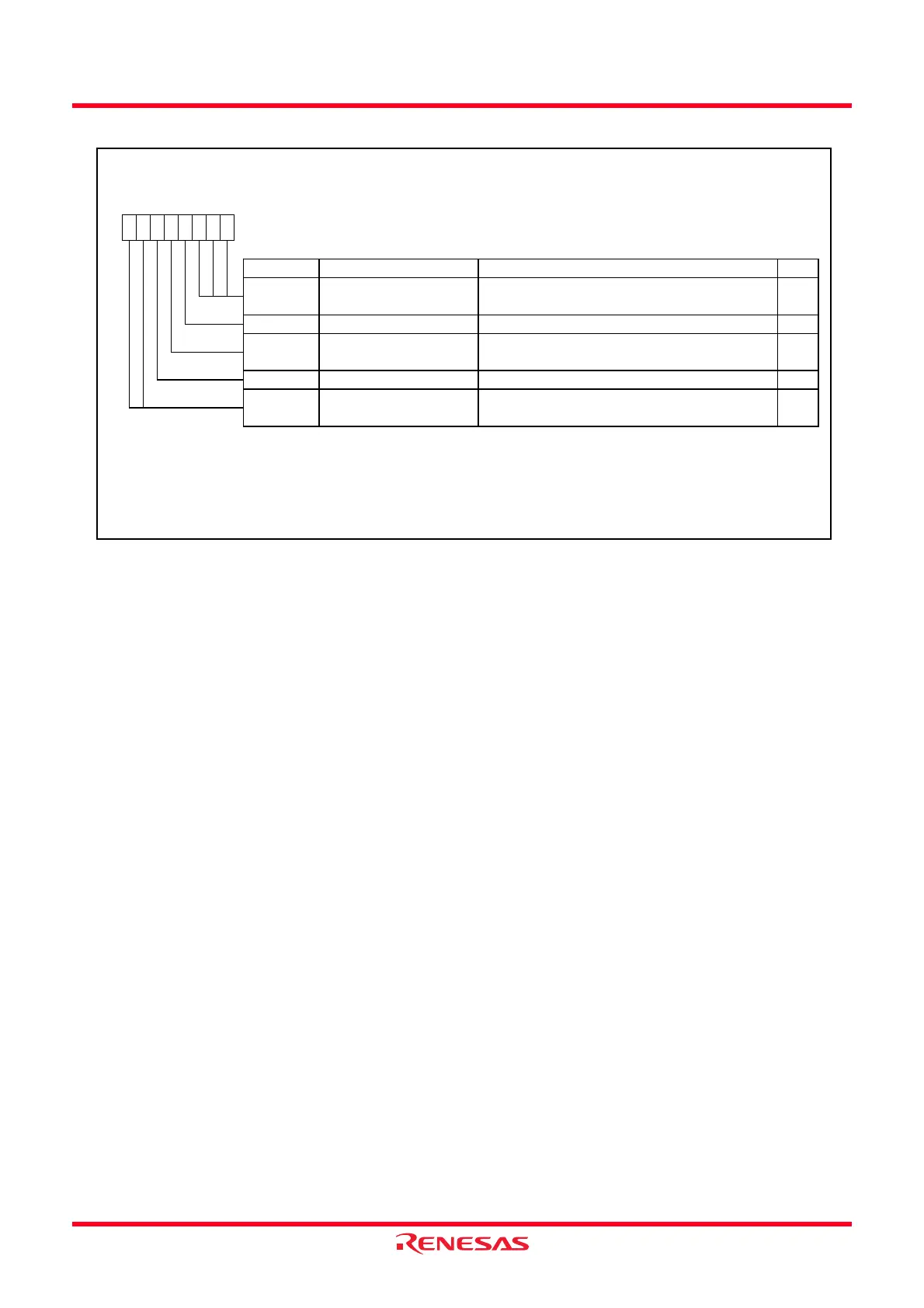
Figure 18.7 ADCON1 Register in Repeat Mode
A/D Control Register 1
(1)
Symbol Address After Reset
ADCON1
00D7h 00h
Bit Symbol Bit Name Function RW
NOTES:
1.
2.
3. When the VCUT bit is set to 1 (connected) from 0 (not connected), w ait for 1 µs or more before starting A/D
conversion.
b3 b2
VCUT
b1 b0
000
Refer to a description of the CKS0 bit in the
ADCON0 register function
b7 b6 b5 b4
—
(b2-b0)
001 0
BITS RW
If the ADCON1 register is rew ritten during A/D conversion, the conversion result is indeterminate.
CKS1 RW
RW
RW
—
(b7-b6)
Reserved bit
Set the BITS bit to 0 (8-bit mode) in repeat mode.
Vref connect bit
(3)
1 : Vref connected
Reserved bit Set to 0
8/10-bit mode select bit
(2)
0 : 8-bit mode
RW
Set to 0
Frequency select bit 1
 Loading...