R8C/20 Group, R8C/21 Group 10. Clock Generation Circuit
Rev.2.00 Aug 27, 2008 Page 83 of 458
REJ09B0250-0200
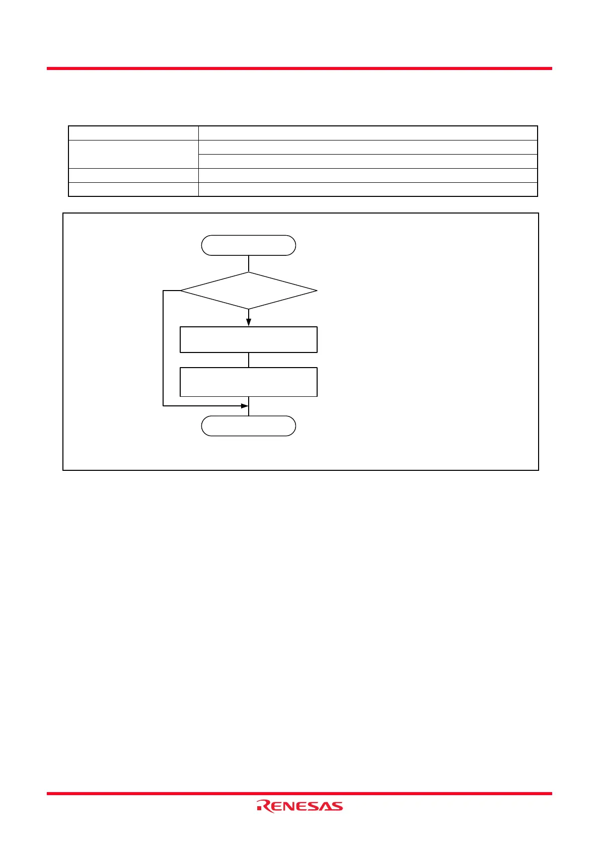
Figure 10.13 Procedure for Switching Clock Source from Low-Speed On-Chip Oscillator to XIN
Clock
Table 10.6 Determining Interrupt Source for Oscillation Stop Detection, Watchdog Timer,
Voltage Monitor 1, and Voltage Monitor 2 Interrupts
Generated Interrupt Source Bit Showing Interrupt Cause
Oscillation Stop Detection
((a) or (b))
(a) OCD3 bit in OCD register = 1
(b) OCD1 to OCD0 bits in OCD register = 11b and the OCD2 bit = 1
Watchdog Timer VW2C3 bit in VW2C register = 1
Voltage Monitor 2 VW2C2 bit in VW2C register = 1
Set OCD1 to OCD0 bits to 00b
Determine several times
that the OCD bit is 0 (XIN clock
oscillates)
Yes
Set OCD2 bit to 0
(select XIN Clock)
End
Switch to XIN clock
OCD3 to OCD0 bits: Bits in OCD register
No
 Loading...