RL78/G13 CHAPTER 29 ELECTRICAL SPECIFICATIONS
R01UH0146EJ0100 Rev.1.00 1008
Sep 22, 2011
Caution The pins mounted depend on the product. Refer to 2.1.1 20-pin products to 2.1.14 128-pin products,
and 2.1.15 Pins for each product (pins other than port pins).
29.6 Peripheral Functions Characteristics
29.6.1 Serial array unit
(1) During communication at same potential (UART mode) (dedicated baud rate generator output)
(T
A = −40 to +85°C, 1.6 V ≤ EVDD0 = EVDD1 ≤ VDD ≤ 5.5 V, VSS = EVSS0 = EVSS1 = 0 V)
Parameter Symbol Conditions MIN. TYP. MAX. Unit
fMCK/6
Note 2
bps Transfer rate
Note 1
Theoretical value of the
maximum transfer rate
f
CLK = 32 MHz, fMCK = fCLK
5.3 Mbps
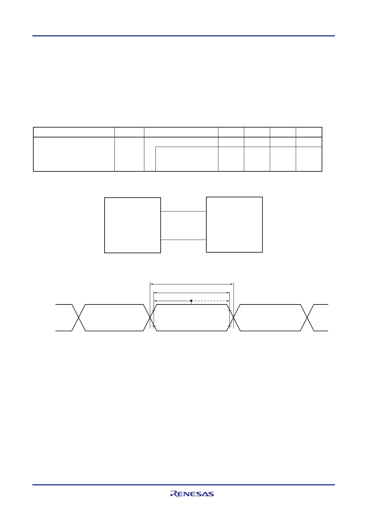
UART mode connection diagram (during communication at same potential)
User's device
TxDq
RxDq
Rx
Tx
RL78/G13
UART mode bit width (during communication at same potential) (reference)
Baud rate error tolerance
High-/Low-bit width
1/Transfer rate
TxDq
RxDq
Notes 1. Transfer rate in the SNOOZE mode is max. 9600 bps, min. 4800 bps.
2. The following conditions are required for low voltage interface when E
VDD0<VDD.
2.4 V ≤ EV
DD0 < 2.7 V : MAX. 2.6 Mbps
1.8 V ≤ EV
DD0 < 2.4 V : MAX. 1.3 Mbps
1.6 V ≤ EVDD0 < 1.8 V : MAX. 0.6 Mbps
Caution Select the normal input buffer for the RxDq pin and the normal output mode for the TxDq pin by using
port input mode register g (PIMg) and port output mode register g (POMg).
Remarks 1. q: UART number (q = 0 to 3), g: PIM and POM number (g = 0, 1, 8, 14)
2. f
MCK: Serial array unit operation clock frequency
(Operation clock to be set by the CKSmn bit of serial mode register mn (SMRmn). m: Unit number,
n: Channel number (mn = 00 to 03, 10 to 13))
<R>
<R>

 Loading...


