RL78/G13 CHAPTER 29 ELECTRICAL SPECIFICATIONS
R01UH0146EJ0100 Rev.1.00 1037
Sep 22, 2011
Caution The pins mounted depend on the product. Refer to 2.1.1 20-pin products to 2.1.14 128-pin products,
and 2.1.15 Pins for each product (pins other than port pins).
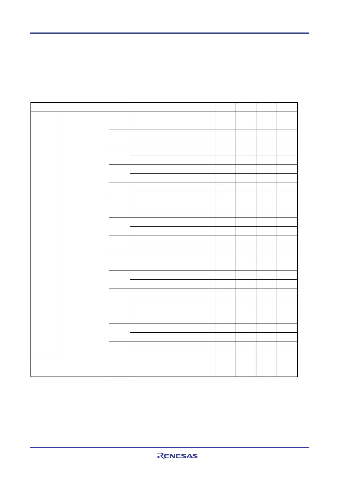
29.7.4 LVD circuit characteristics
LVD Detection Voltage of Reset Mode and Interrupt Mode
(T
A = −40 to +85°C, VPDR ≤ EVDD0 = EVDD1 ≤ VDD ≤ 5.5 V, VSS = EVSS0 = EVSS1 = 0 V)
Parameter Symbol Conditions MIN. TYP. MAX. Unit
Power supply rise time 3.98 4.06 4.14
V
VLVD0
Power supply fall time 3.90 3.98 4.06
V
Power supply rise time 3.68 3.75 3.82
V
VLVD1
Power supply fall time 3.60 3.67 3.74
V
Power supply rise time 3.07 3.13 3.19
V
VLVD2
Power supply fall time 3.00 3.06 3.12
V
Power supply rise time 2.96 3.02 3.08
V
VLVD3
Power supply fall time 2.90 2.96 3.02
V
Power supply rise time 2.86 2.92 2.97
V
VLVD4
Power supply fall time 2.80 2.86 2.91
V
Power supply rise time 2.76 2.81 2.87
V
VLVD5
Power supply fall time 2.70 2.75 2.81
V
Power supply rise time 2.66 2.71 2.76
V
VLVD6
Power supply fall time 2.60 2.65 2.70
V
Power supply rise time 2.56 2.61 2.66
V
VLVD7
Power supply fall time 2.50 2.55 2.60
V
Power supply rise time 2.45 2.50 2.55
V
VLVD8
Power supply fall time 2.40 2.45 2.50
V
Power supply rise time 2.05 2.09 2.13
V
VLVD9
Power supply fall time 2.00 2.04 2.08
V
Power supply rise time 1.94 1.98 2.02
V
VLVD10
Power supply fall time 1.90 1.94 1.98
V
Power supply rise time 1.84 1.88 1.91
V
VLVD11
Power supply fall time 1.80 1.84 1.87
V
Power supply rise time 1.74 1.77 1.81
V
VLVD12
Power supply fall time 1.70 1.73 1.77
V
Power supply rise time 1.64 1.67 1.70
V
Detection
voltage
Supply voltage level
V
LVD13
Power supply fall time 1.60 1.63 1.66
V
Minimum pulse width tLW
300
μ
s
Detection delay time tLD
300
μ
s
Remark V
LVD(n − 1) > VLVDn: n = 1 to 13

 Loading...


