RL78/G13 CHAPTER 9 CLOCK OUTPUT/BUZZER OUTPUT CONTROLLER
R01UH0146EJ0100 Rev.1.00 462
Sep 22, 2011
CHAPTER 9 CLOCK OUTPUT/BUZZER OUTPUT CONTROLLER
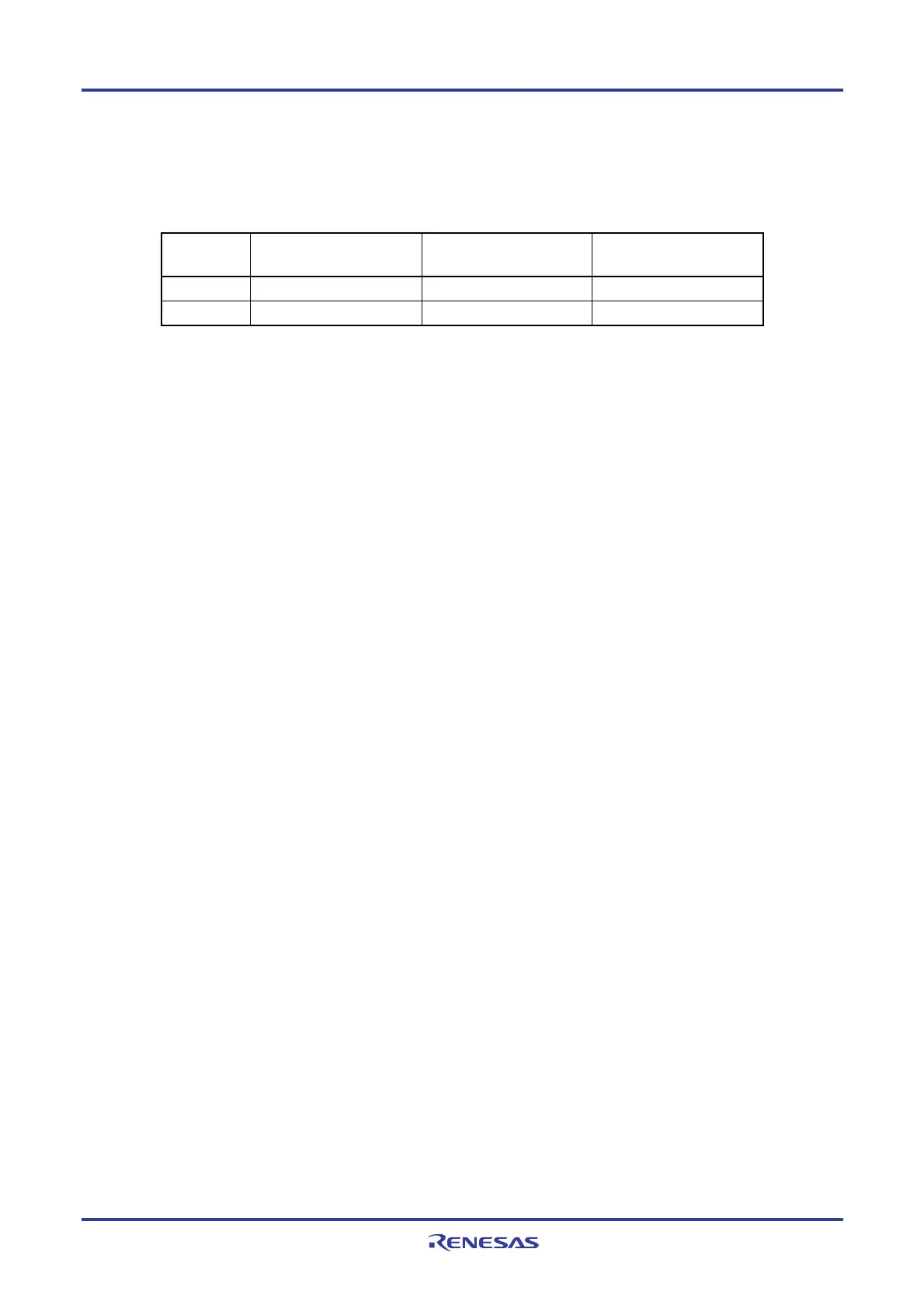
The number of output pins of the clock output and buzzer output controllers differs, depending on the product.
Output pin 20-pin 24, 25-pin
30, 32, 36, 40, 44, 48, 52,
64, 80, 100, 128-pin
PCLBUZ0
− √ √
PCLBUZ1
− − √
Caution Most of the following descriptions in this chapter use the 64-pin as an example.
9.1 Functions of Clock Output/Buzzer Output Controller
The clock output controller is intended for carrier output during remote controlled transmission and clock output for
supply to peripheral ICs.
Buzzer output is a function to output a square wave of buzzer frequency.
One pin can be used to output a clock or buzzer sound.
Two output pins, PCLBUZ0 and PCLBUZ1, are available.
The PCLBUZn pin outputs a clock selected by clock output select register n (CKSn).
Figure 9-1 shows the block diagram of clock output/buzzer output controller.
Caution In the low-consumption RTC mode (when the RTCLPC bit of the operation speed mode control
register (OSMC) = 1), it is not possible to output the subsystem clock (f
SUB) from the PCLBUZn pin.
Remark n = 0, 1

 Loading...


