RL78/G13 CHAPTER 1 OUTLINE
R01UH0146EJ0100 Rev.1.00 19
Sep 22, 2011
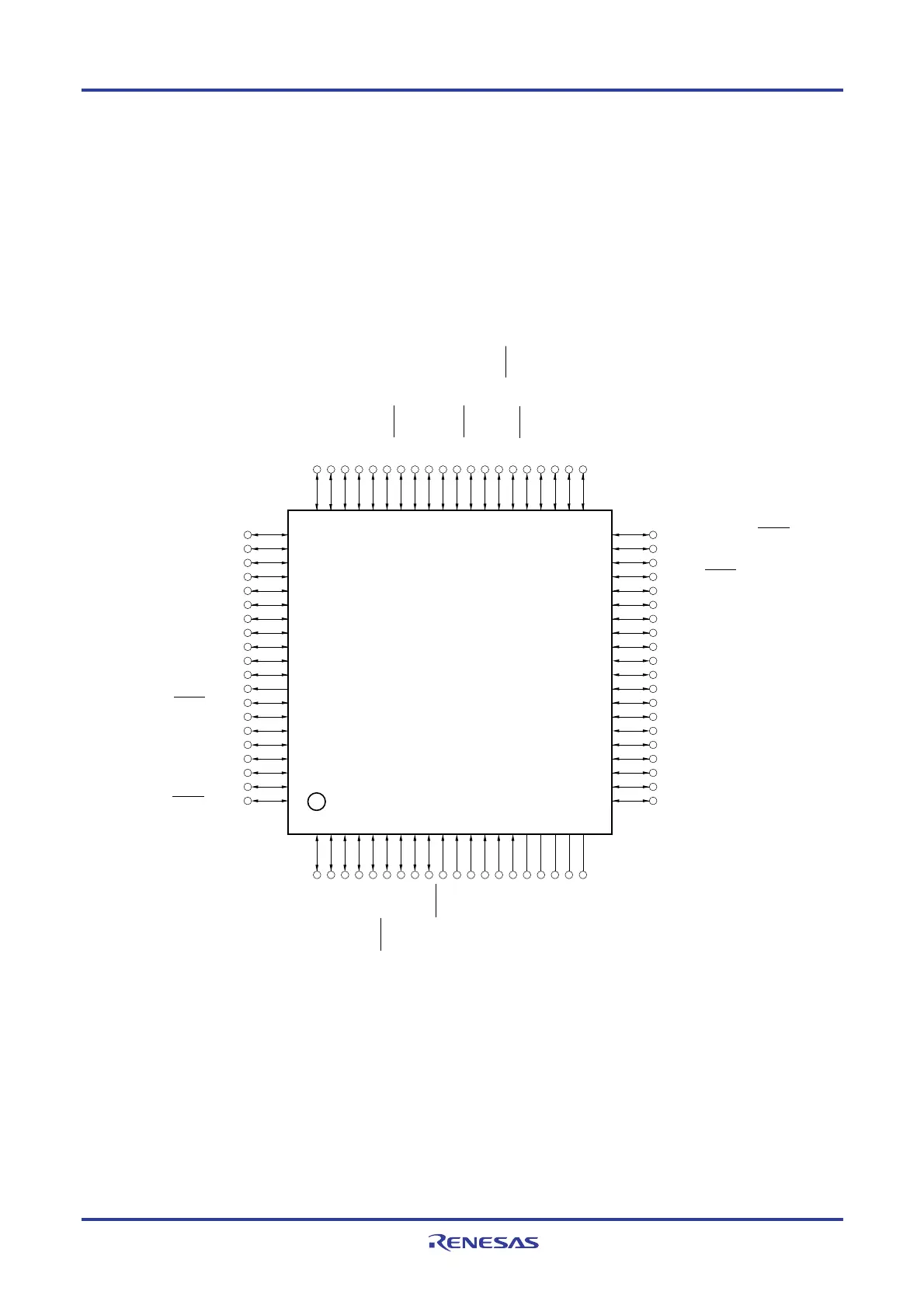
1.3.12 80-pin products
• 80-pin plastic LQFP (14 × 14)
• 80-pin plastic LQFP (fine pitch) (12 × 12)
P152/ANI10
P151/ANI9
P150/ANI8
P27/ANI7
P26/ANI6
P25/ANI5
P24/ANI4
P23/ANI3
P22/ANI2
P21/ANI1/AV
REFM
P20/ANI0/AV
REFP
P130
P04/SCK10/SCL10
P03/ANI16/SI10/RxD1/SDA10
P02/ANI17/SO10/TxD1
P01/TO00
P00/TI00
P144/SO30/TxD3
P143/SI30/RxD3/SDA30
P142/SCK30/SCL30
P153/ANI11
P100/ANI20
P147/ANI18
P146
P111/(INTP11)
P110/(INTP10)
P10/SCK00/SCL00/(TI07)/(TO07)
P11/SI00/RxD0/TOOLRxD/SDA00/(TI06)/(TO06)
P12/SO00/TxD0/TOOLTxD/(INTP5)/(TI05)/(TO05)
P13/TxD2/SO20/(SDAA0)/(TI04)/(TO04)
P14/RxD2/SI20/SDA20/(SCLA0)/(TI03)/(TO03)
P15/SCK20/SCL20/(TI02)/(TO02)
P16/TI01/TO01/INTP5/(SI00)/(RXD0)
P17/TI02/TO02/(SO00)/(TXD0)
P55/(PCLBUZ1)/(SCK00)
P54/SCK31/SCL31
P53/SI31/SDA31
P52/SO31
P51/INTP2/SO11
P50/INTP1/SI11/SDA11
1 2 3 4 5 6 7 8 9 10 11 12 13 14 15 16 17 18 19 20
60 59 58 57 56 55 54 53 52 51 50 49 48 47 46 45 44 43 42 41
P30/INTP3/RTC1HZ/SCK11/SCL11
P05/TI05/TO05
P06/TI06/TO06
P70/KR0/SCK21/SCL21
P71/KR1/SI21/SDA21
P72/KR2/SO21
P73/KR3
P74/KR4/INTP8
P75/KR5/INTP9
P76/KR6/INTP10/(RXD2)
P77/KR7/INTP11/(TXD2)
P67/TI13/TO13
P66/TI12/TO12
P65/TI11/TO11
P64/TI10/TO10
P31/TI03/TO03/INTP4/(PCLBUZ0)
P63/SDAA1
P62/SCLA1
P61/SDAA0
P60/SCLA0
P141/PCLBUZ1/INTP7
P140/PCLBUZ0/INTP6
P120/ANI19
P45/SO01
P44/SI01/SDA01
P43/SCK01/SCL01
P42/TI04/TO04
P41/TI07/TO07
P40/TOOL0
RESET
P124/XT2/EXCLKS
P123/XT1
P137/INTP0
P122/X2/EXCLK
P121/X1
REGC
V
SS
EV
SS0
V
DD
EV
DD0
40
39
38
37
36
35
34
33
32
31
30
29
28
27
26
25
24
23
22
21
61
62
63
64
65
66
67
68
69
70
71
72
73
74
75
76
77
78
79
80
Cautions 1. Make EV
SS0 pin the same potential as VSS pin.
2. Make V
DD pin the potential that is higher than EVDD0 pin.
3. Connect the REGC pin to Vss via a capacitor (0.47 to 1
μ
F).
Remarks 1. For pin identification, see 1.4 Pin Identification.
2. When using the microcontroller for an application where the noise generated inside the microcontroller
must be reduced, it is recommended to supply separate powers to the V
DD and EVDD0 pins and connect
the VSS and EVSS0 pins to separate ground lines.
3. Functions in parentheses in the above figure can be assigned via settings in the peripheral I/O redirection
register (PIOR).
<R>

 Loading...


