RL78/G13 CHAPTER 2 PIN FUNCTIONS
R01UH0146EJ0100 Rev.1.00 92
Sep 22, 2011
2.3 Pin I/O Circuits and Recommended Connection of Unused Pins
Table 2-3 shows the types of pin I/O circuits and the recommended connections of unused pins.
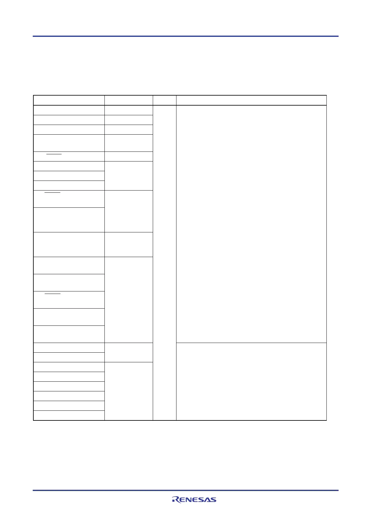
Table 2-3. Connection of Unused Pins (128-pin products) (1/4)
Pin Name I/O Circuit Type
I/O Recommended Connection of Unused Pins
P00/TI00 8-R
P01/TO00 5-AN
P02/ANI17/SO10/TxD1 11-U
P03/ANI16/SI10/RxD1/
SDA10
11-V
P04/SCK10/SCL10 5-AN
P05
P06
P07
8-R
P10/SCK00/SCL00/(TI07)/(T
O07)
P11/SI00/RxD0/
TOOLRxD/SDA00/(TI06)/
(TO06)
5-AN
P12/SO00/TxD0/
TOOLTxD/(INTP5)/(TI05)/
(TO05)
8-R
P13/TxD2/SO20/(SDAA0)/(TI
04)/(TO04)
P14/RxD2/SI20/SDA20/
(SCLA0)/(TI03)/(TO03)
P15/SCK20/SCL20/(TI02)/(T
O02)
P16/TI01/TO01/INTP5/
(SI00)/(RxD0)
P17/TI02/TO02/(SO00)/
(TxD0)
5-AN
Input: Independently connect to EV
DD0, EVDD1 or EVSS0, EVSS1
via a resistor.
Output: Leave open.
P20/ANI0/AVREFP
P21/ANI1/AVREFM
11-T
P22/ANI2
P23/ANI3
P24/ANI4
P25/ANI5
P26/ANI6
P27/ANI7
11-G
I/O
Input: Independently connect to V
DD or VSS via a resistor.
Output: Leave open.
Remarks 1. With products not provided with an EVDD0, EVDD1, EVSS0, or EVSS1 pin, replace EVDD0 and EVDD1 with VDD, or
replace EV
SS0 and EVSS1 with VSS.
2. Functions in parentheses in the above figure can be assigned via settings in the peripheral I/O redirection
register (PIOR).
<R>

 Loading...


