RL78/G13 CHAPTER 25 FLASH MEMORY
R01UH0146EJ0100 Rev.1.00 933
Sep 22, 2011
The dedicated flash memory programmer generates the following signals for the RL78/G13. See the manual of PG-FP5,
FL-PR5, or E1 on-chip debugging emulator for details.
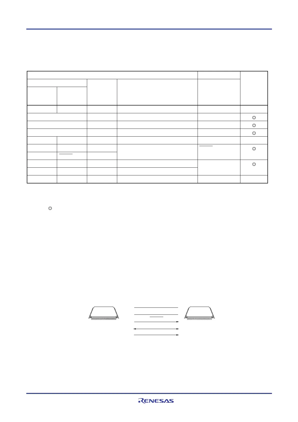
Table 25-2. Pin Connection
Dedicated Flash Memory Programmer RL78/G13 Connection
Signal Name
PG-FP5,
FL-PR5
E1 on-chip
debugging
emulator
I/O Pin Function Pin Name
FLMD0
−
Output Mode signal
− ×
VDD I/O VDD voltage generation/power monitoring VDD
GND
−
Ground
V
SS, EVSS, REGC
Note
EMVDD
−
Driving power for TOOL pin VDD, EVDD
CLK
−
Output Clock output
− ×
/RESET
−
Output
−
RESET Output
Reset signal RESET
−
TOOL0 I/O Transmit/receive signal TOOL0
SI/RxD
−
I/O Transmit/receive signal
SCK
−
Output Transfer clock
− ×
Note Connect REGC pin to ground via a capacitor (default: 0.47
μ
F).
Remark
: Be sure to connect the pin.
×: The pin does not have to be connected.
25.2 Writing to Flash Memory by Using External Device (that Incorporates UART)
On-board data writing to the internal flash memory is possible by using the RL78/G13 and an external device (a
microcontroller or ASIC) connected to a UART.
25.2.1 Programming Environment
The environment required for writing a program to the flash memory of the RL78/G13 is illustrated below.
Figure 25-3. Environment for Writing Program to Flash Memory
RL78/G13External device
(such as microcontroller
and ASIC)
V
DD, EVDD
VSS, EVSS
RESET
UART (TOOLTxD, TOOLRxD)
TOOL0
Processing to write data to or delete data from the RL78/G13 by using an external device is performed on-board. Off-
board writing is not possible.

 Loading...


