RL78/F13, F14 CHAPTER 35 ELECTRICAL SPECIFICATIONS (GRADE K)
R01UH0368EJ0210 Rev.2.10 1752
Dec 10, 2015
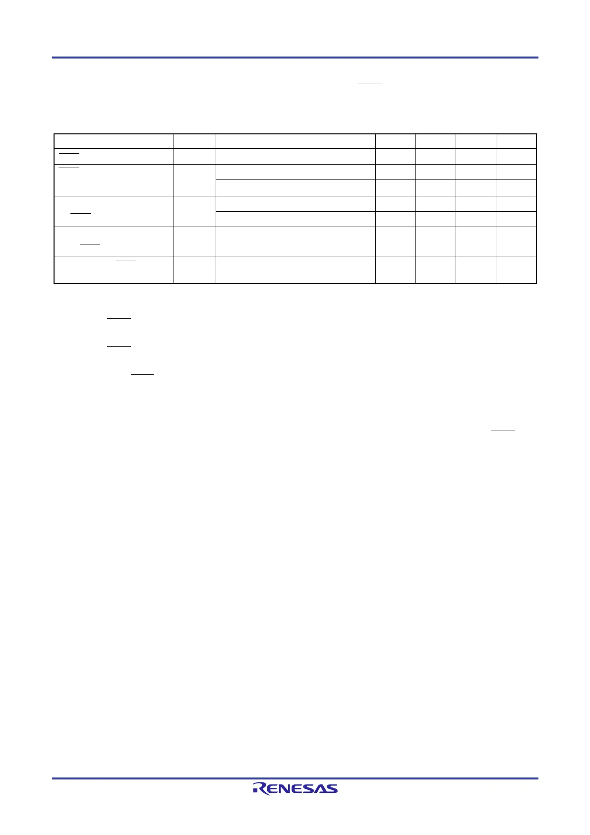
(2) During communication at same potential (CSI mode) (master mode, SCKp … internal clock output, normal
slew rate)
(TA = -40 to +125C, 2.7 V EVDD0 = EVDD1 = VDD 5.5 V, VSS = EVSS0 = EVSS1 = 0 V)
Parameter Symbol Conditions MIN. TYP. MAX. Unit
SCKp cycle time
t
KCY1 166.6
Note 5
ns
SCKp high-level width, low-
level width
t
KH1,
tKL1
4.0 V EVDD0 5.5 V
t
KCY1
/2 – 12
ns
2.7 V EVDD0 4.0 V
t
KCY1
/2 – 18
ns
SIp setup time
(to SCKp)
Note 1
t
SIK1 4.0 V EVDD0 5.5 V 55 ns
2.7 V EVDD0 4.0 V 66 ns
SIp hold time
(from SCKp)
Note 2
t
KSI1 30 ns
Delay time from SCKp to
SOp output
Note 3
t
KSO1 C = 30 pF
Note 4
40 ns
Notes 1. When DAPmn = 0 and CKPmn = 0, or DAPmn = 1 and CKPmn = 1. The Slp setup time becomes "to
SCKp" when DAPmn = 0 and CKPmn = 1 or DAPmn = 1 and CKPmn = 0.
2. When DAPmn = 0 and CKPmn = 0 or DAPmn = 1 and CKPmn = 1. The SIp hold time becomes "from
SCKp" when DAPmn = 0 and CKPmn = 1 or DAPmn = 1 and CKPmn = 0.
3. When DAPmn = 0 and CKPmn = 0, or DAPmn = 1 and CKPmn = 1. The delay time to SOp output becomes
“from SCKp” when DAPmn = 0 and CKPmn = 1, or DAPmn = 1 and CKPmn = 0.
4. C is the load capacitance of the SCKp and SOp output lines.
5. t
KCY1 4/fCLK must also be satisfied.
Caution Select the normal input buffer for the SIp pin and normal output mode for the SOp pin and SCKp pin.
Remark p: CSIp (p = 00, 01, 10, 11), m: Unit m (m = 0, 1), n: Channel n (n = 0, 1)
 Loading...


