MB95630H Series
152 FUJITSU SEMICONDUCTOR LIMITED MN702-00009-2v0-E
CHAPTER 11 8/16-BIT COMPOSITE TIMER
11.10 Operation of PWM Timer Function
(Variable-cycle Mode)
11.10 Operation of PWM Timer Function
(Variable-cycle Mode)
This section describes the operation of the PWM timer function (variable-cycle
mode) of the 8/16-bit composite timer.
■ Operation of PWM Timer Function (Variable-cycle Mode)
To use the PWM timer function (variable-cycle mode), do the settings shown in Figure
11.10-1.
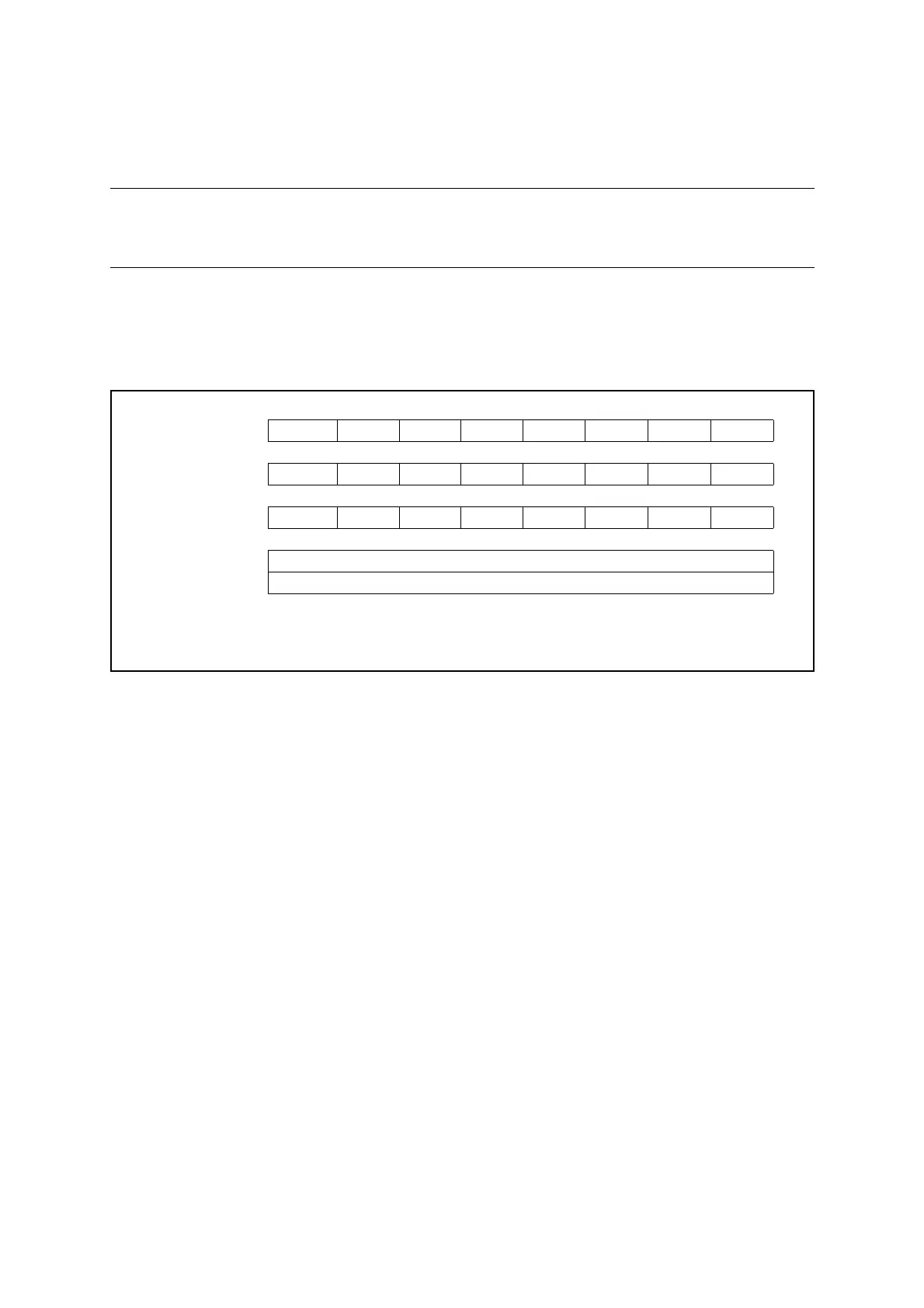
Figure 11.10-1 Settings for PWM Timer Function (Variable-cycle Mode)
As for the PWM timer function (variable-cycle mode), both timers n0 and n1 are used. PWM
signal of any cycle and of any duty is output from the timer output pin (TOn0). The cycle is
specified by the 8/16-bit composite timer n1 data register (Tn1DR), and the "L" pulse width is
specified by the 8/16-bit composite timer n0 data register (Tn0DR).
Since both the 8-bit counters are used for this function, the composite timer cannot form a
16-bit counter.
Enabling timer operation (Tn0CR1/Tn1CR1:STA = 1) sets the mode bit (TMCRn:MOD) to
"0". As the first cycle always begins with "L" pulse output, the timer initial value setting bit
(Tn0CR1/Tn1CR1:SO) has no effect on operation.
An interrupt flag (Tn0CR1/Tn1CR1:IF) is set when the 8-bit counter corresponding to that
interrupt flag matches the value in its corresponding 8/16-bit composite timer data register
(Tn0DR/Tn1DR).
The 8/16-bit composite timer data register value is transferred to the temporary storage latch
(comparison data storage latch) in the comparator either when the counter starts counting or
when a comparison match with each counter value is detected.
"H" is not output when the "L" pulse width setting value is greater than the cycle setting value.
The count clock must be selected for both timers n0 and n1. Selecting different count clocks
for the two timers is prohibited.
When the timer stops operating, the timer output bit (TMCRn:TO0) holds the last output value.
If the 8/16-bit composite timer data register is modified during operation, the data written will
become valid from the cycle immediately after the detection of a synchronous match.
bit7 bit6 bit5 bit4 bit3 bit2 bit1 bit0
Tn0CR0/Tn1CR0 IFE C2 C1 C0 F3 F2 F1 F0
❍❍❍❍0100
Tn0CR1/Tn1CR1 STA HO IE IR BF IF SO OE
1 ❍❍ ××❍ ××
TMCRn TO1 TO0 TIS MOD FE11 FE10 FE01 FE00
❍❍××❍❍❍❍
Tn0DR Sets "L" pulse width (compare value)
Tn1DR Sets the cycle of PWM waveform (compare value)
❍: Bit to be used
×: Unused bit
1: Set to "1"
0: Set to "0"
 Loading...

