MB95630H Series
MN702-00009-2v0-E FUJITSU SEMICONDUCTOR LIMITED 381
CHAPTER 21 MULTI-PULSE GENERATOR
21.2 Block Diagram
21.2 Block Diagram
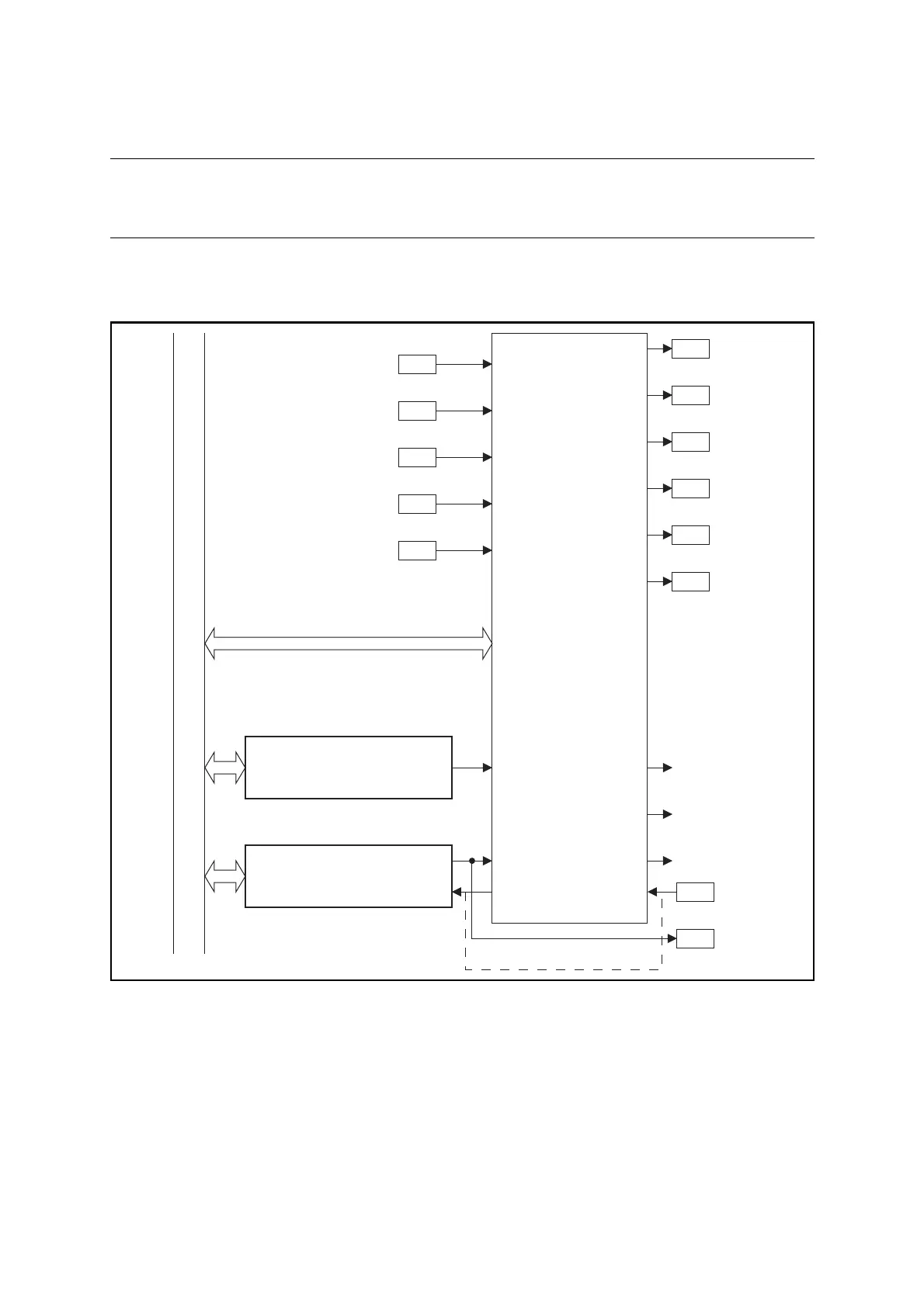
Figure 21.2-1 shows the block diagram of the multi-pulse generator and
Figure 21.2-2 the block diagram of the waveform sequencer.
■ Block Diagram of Multi-pulse Generator
Figure 21.2-1 Block Diagram of Multi-pulse Generator
*1: The dotted line represents the TI1 path. The 16-bit reload time can be used independently of the multi-
pulse generator.
*2: See "■ Multi-pulse Generator Interrupt Sources" in "21.4 Interrupts".
● 16-bit PPG timer
The 16-bit PPG timer is used to provide the PPG signal for the waveform sequencer. Details of
the 16-bit PPG timer are described in "CHAPTER 19 16-BIT PPG TIMER".
DTTI
SNI2
SNI1
SNI0
TIN0
OPT5
OPT4
OPT3
OPT2
OPT1
OPT0
WAVEFORM
SEQUENCER
Pin
Pin
Pin
Pin
PPG1
Pin
Pin
Pin
Pin
Pin
Pin
Pin
16-BIT PPG TIMER
PPG1
WTIN0
16-BIT RELOAD TIMER
F
2
MC-8FX Bus
TOUT
TIN0O
TIN
OPT5
OPT4
OPT3
OPT2
OPT1
DTTI
SNI2
SNI1
SNI0
TI1
OPT0
Pin
TI1
Pin
TO1
Interrupt A
*
2
Interrupt A
Interrupt B
*
2
Interrupt B
Interrupt C
*
2
Interrupt C
*1
 Loading...

