MB95630H Series
MN702-00009-2v0-E FUJITSU SEMICONDUCTOR LIMITED 265
CHAPTER 15 8/10-BIT A/D CONVERTER
15.2 Configuration
15.2 Configuration
The 8/10-bit A/D converter consists of the following blocks:
• Clock selector (input clock selector for starting A/D conversion)
• Analog channel selector
• Sample-and-hold circuit
• Control circuit
• 8/10-bit A/D converter data register (upper/lower) (ADDH/ADDL)
• 8/10-bit A/D converter control register 1 (ADC1)
• 8/10-bit A/D converter control register 2 (ADC2)
The number of analog input pins and that of analog channels of the 8/10-bit A/D converter vary
among products. For details, refer to the device data sheet.
In this chapter, "n" in a pin name represents the analog input pin number.
For details of pin
names of a product, refer to the device data sheet.
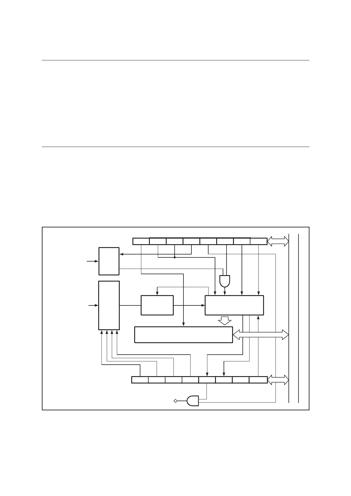
■ Block Diagram of 8/10-bit A/D Converter
Figure 15.2-1 is the block diagram of the 8/10-bit A/D converter.
Figure 15.2-1 Block Diagram of 8/10-bit A/D Converter
● Clock selector
This selects the A/D conversion clock with continuous activation having been enabled
(ADC2:EXT = 1).
AD8 TIM1 TIM0 ADCK ADIE EXT
CKDIV1 CKDIV0
ANS3 ANS2ANS1ANS0 ADI ADMV
Reserved
AD
8/10-bit A/D converter control register 2 (ADC2)
Analog
channel
selector
8/10-bit A/D converter control register 1 (ADC1)
Sample-
and-hold
circuit
Control circuit
8/10-bit A/D converter data register(upper/lower)
(ADDH/ADDL)
IRQ
Internal data bus
ANn
8/16-bit
composite timer
output pin (TO00)
Startup
signal
selector
 Loading...

