MB95630H Series
404 FUJITSU SEMICONDUCTOR LIMITED MN702-00009-2v0-E
CHAPTER 21 MULTI-PULSE GENERATOR
21.5 Operations
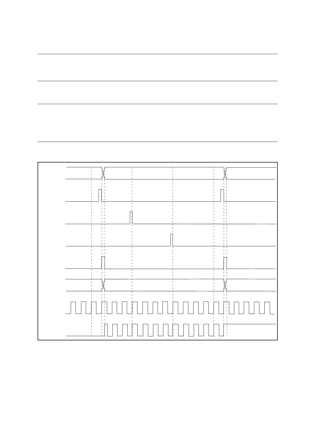
21.5.4.1 At OPDBRH0 and OPDBRL0 Write
The timing change of the output pin OPTx, which is triggered by OPDBRH0 and
OPDBRL0 write, is shown in Figure 21.5-13.
■ Timing Generated by OPDBRH0 and OPDBRL0 Write (OPS[2:0] = 0b000)
Note:
Word access to the output data buffer register 0 must be used in this operation, byte
access to either lower register or upper register does not start any transfer operation. The
reload timer is free to be used in this operation mode.
Figure 21.5-13 Timing Generated by OPDBRH0 and OPDBRL0 Write (OPS[2:0] = 0b000)
OP0[1:0]
(OPDLR)
PPG
OPT0
0b00 0b01 0b11
0b1100b000 0b001
WTO
RDA[2:0]
(OPDUR)
ODBR2W
ODBR1W
ODBR0W
 Loading...

