MB95630H Series
6 FUJITSU SEMICONDUCTOR LIMITED MN702-00009-2v0-E
CHAPTER 2 CPU
2.1 Dedicated Registers
2.1.1 Register Bank Pointer (RP)
The register bank pointer (RP) in bit15 to bit11 of the program status (PS)
register contains the address of the general-purpose register bank that is
currently in use and is translated into a real address when general-purpose
register addressing is used.
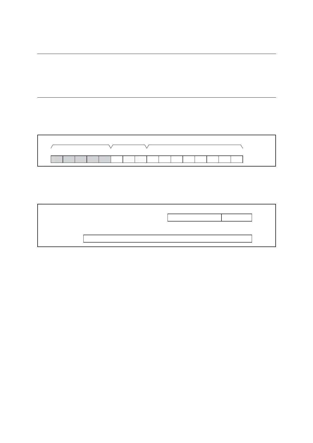
■ Configuration of Register Bank Pointer (RP)
Figure 2.1-2 shows the configuration of the register bank pointer.
Figure 2.1-2 Configuration of Register Bank Pointer
The register bank pointer contains the address of the register bank currently in use. The content
of the register bank pointer is translated into a real address according to the rule shown in
Figure 2.1-3.
Figure 2.1-3 Rule for Translation into Real Addresses in General-purpose Register Area
The register bank pointer specifies the register bank used as general-purpose registers in the
RAM area. There are a total of 32 register banks, which are specified by setting a value
between 0 and 31 in the upper five bits of the register bank pointer. Each register bank has
eight 8-bit general-purpose registers which are selected by the lower three bits of the op-code.
The register bank pointer allows the space from "0x0100" to "0x01FF"(max) to be used as a
general-purpose register area. However, certain products have restrictions on the size of the
area available for the general-purpose register area. The initial value of the register bank
pointer after a reset is "0x0000".
■ Mirror Address for Register Bank and Direct Bank Pointer
Values can be written to the register bank pointer (RP) and the direct bank pointer (DP) by
accessing the program status (PS) register with the "MOVW PS,A" instruction; the two
pointers can be read by accessing PS with the "MOVW A,PS" instruction. Values can also be
directly written to and read from the two pointers by accessing "0x0078", the mirror address of
the register bank pointer.
CCRDPRP
PS 0b00000
RP
initial value
R4 R3 R2 R1 R0 DP2 DP1 DP0 H I IL1 IL0 N Z V C
bit15 bit14 bit13bit12 bit11 bit10 bit9 bit8bit7 bit6 bit5 bit4 bit3bit2 bit1 bit0
↓↓↓↓↓↓↓↓↓↓↓↓↓↓↓↓
“0” “0”
A15 A14 A13 A12 A11 A10 A9 A8 A7 A6 A5 A4 A3 A2 A1 A0
“0” “0” “0” “0” “0” “1” R4 R3 R2 R1 R0 b2 b1 b0
Generated
address
Fixed value RP: Upper Op-code: Lower