EasyManua.ls Logo

Fujitsu 8FX User Manual

Fujitsu 8FX
650 pages
To Next Page IconTo Next Page
To Previous Page IconTo Previous Page
Page #483 background imageLoading...
Page #483 background image
MB95630H Series
MN702-00009-2v0-E FUJITSU SEMICONDUCTOR LIMITED 461
CHAPTER 22 UART/SIO
22.5 Interrupts
22.5 Interrupts
The UART/SIO has six interrupt-related bits: receive error flag bits (PER, OVE,
FER), receive data register full flag bit (RDRF), transmit data register empty flag
bit (TDRE), and transmission completion flag bit (TCPL).
â–  Interrupts of UART/SIO
Table 22.5-1 lists the UART/SIO interrupt control bits and interrupt sources.
â–  Transmit Interrupt
When transmit data is written to the UART/SIO serial output data register ch. n (TDRn), the
data is transferred to the transmission shift register. When the next piece of data can be written,
the TDRE bit is set to "1". At this time, an interrupt request to the interrupt controller occurs
when transmit data register empty interrupt enable bit has been enabled (SMC2n:TEIE = 1).
The TCPL bit is set to "1" upon completion of transmission of all pieces of transmit data. At
this time, an interrupt request to the interrupt controller occurs when transmission completion
interrupt enable bit has been enabled (SMC2n:TCIE = 1).
â–  Receive Interrupt
If the data is input successfully up to the stop bit, the RDRF bit is set to "1". If an overrun
error, a parity error, or a framing error occurs, the corresponding error flag bit (PER, OVE, or
FER) is set to "1".
These bits are set when a stop bit is detected. If receive interrupt enable bit has been enabled
(SMC2n:RIE = 1), an interrupt request to the interrupt controller will be generated.
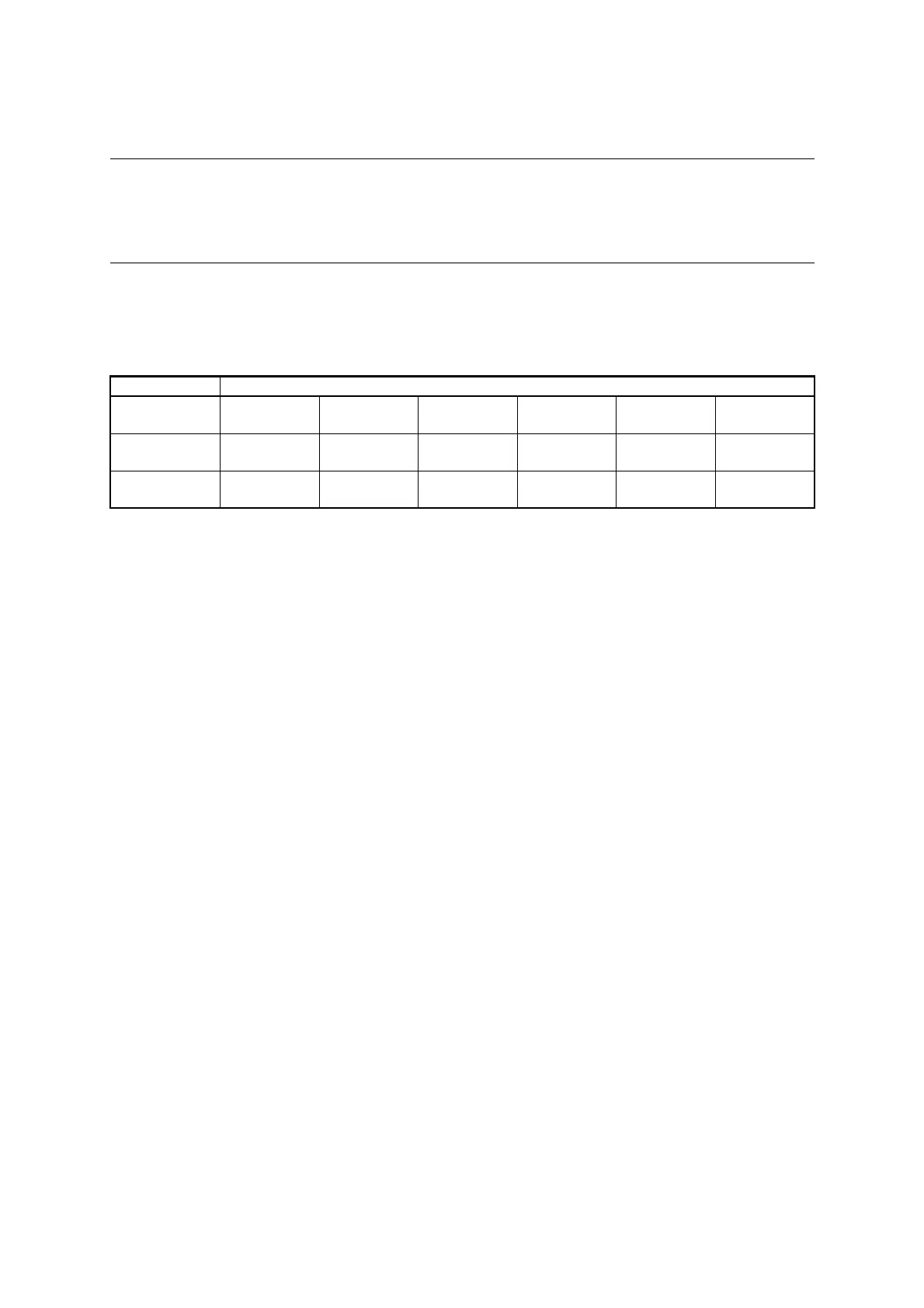
Table 22.5-1 UART/SIO Interrupt Control Bits and Interrupt Sources
Item Description
Interrupt request
flag bit
SSRn:TDRE SSRn:TCPL SSRn:RDRF SSRn:PER SSRn:OVE SSRn:FER
Interrupt request
enable bit
SMC2n:TEIE SMC2n:TCIE SMC2n:RIE SMC2n:RIE SMC2n:RIE SMC2n:RIE
Interrupt source
Transmit data
register empty
Transmission
completion
Receive data full Parity error Overrun error Framing error

Table of Contents

Question and Answer IconNeed help?

Do you have a question about the Fujitsu 8FX and is the answer not in the manual?

Fujitsu 8FX Specifications

General IconGeneral
BrandFujitsu
Model8FX
CategoryComputer Hardware
LanguageEnglish

Summary

PREFACE

The Purpose and Intended Readership of This Manual

Describes the manual's goal, target audience, and general information about the MB95630H Series microcontrollers.

Trademark

Information regarding company and brand names, which are trademarks or registered trademarks of their respective owners.

Sample Programs

Provides information on free sample programs for peripheral resources of the New 8FX family of microcontrollers.

How to Use This Manual

Finding a Function

Explains methods for searching for function details, including CONTENTS and register searches.

Chapters

Briefly describes the structure of the manual, where each chapter explains one peripheral function.

Terminology

Lists and defines terminology used within the manual, such as Word and Byte definitions.

Notations

Explains notations used in the 'Register Configuration' section, covering bits, fields, attributes, and initial values.

CHAPTER 1 MEMORY ACCESS MODE

1.1 Memory Access Mode

Details the single-chip memory access mode supported by the MB95630H Series, including mode data settings.

CHAPTER 2 CPU

2.1 Dedicated Registers

Describes the CPU's dedicated registers, including PC, Accumulator, Temporary Accumulator, Index Register, Extra Pointer, Stack Pointer, and Program Status.

2.2 General-purpose Register

Explains the general-purpose registers, their configuration, features, and usage in interrupt handling and sub-routine calls.

2.3 Placement of 16-bit Data in Memory

Explains how 16-bit data is stored in memory, including states in RAM, specified by operands, and in the stack.

CHAPTER 3 CLOCK CONTROLLER

3.1 Overview

Provides a general overview of the clock controller, its functions, and supported clocks.

3.3 Registers

Details the various registers associated with the clock controller, such as SYCC, PLLC, WATR, STBC, SYCC2, and STBC2.

3.4 Clock Modes

Describes the five available clock modes: main clock, main CR clock, main CR PLL clock, subclock, and sub-CR clock modes.

3.5 Operations in Low Power Consumption Mode (Standby Mode)

Explains the operations in low power consumption modes, including sleep, stop, time-base timer, and watch modes.

CHAPTER 4 RESET

4.1 Reset Operation

Explains the CPU's behavior during reset, including reset sources and the reset operation flow.

4.2 Register

Details the registers related to reset operations, specifically the Reset Source Register (RSRR).

4.3 Notes on Using Reset

Provides important notes and considerations for using the reset functionality, including register initialization.

CHAPTER 5 INTERRUPTS

5.1 Interrupts

Provides an overview of the interrupt system, detailing interrupt request inputs, levels, and interrupt processing.

5.1.2 Interrupt Processing

Explains the step-by-step procedure for processing interrupts, including interrupt controller actions and CPU response.

5.1.3 Nested Interrupts

Discusses the concept of nested interrupts and how they are handled based on interrupt priority levels.

5.1.4 Interrupt Processing Time

Details the time required for interrupt processing, including sampling wait time and interrupt handling time.

CHAPTER 6 I/O PORT

6.1 Overview

Provides a general overview of the I/O port functionality for controlling general-purpose I/O pins.

6.2 Configuration and Operations

Details the configuration and operations of I/O ports, covering their elements and usage as input, output, or peripheral function pins.

CHAPTER 7 TIME-BASE TIMER

7.1 Overview

Provides an overview of the time-base timer, its operating modes, and its interval timer function.

7.2 Configuration

Details the configuration of the time-base timer, including its constituent blocks and input/output clocks.

7.5 Register

Lists and describes the registers associated with the time-base timer, specifically the Time-base Timer Control Register (TBTC).

7.6 Notes on Using Time-base Timer

Provides notes and considerations for using the time-base timer, including interrupt handling and clearing mechanisms.

CHAPTER 9 WATCH PRESCALER

9.1 Overview

Provides an overview of the watch prescaler, a 16-bit down-counting free-run counter with an interval timer function.

9.2 Configuration

Details the configuration of the watch prescaler, including its constituent blocks and input/output clocks.

9.5 Register

Lists the registers associated with the watch prescaler, specifically the Watch Prescaler Control Register (WPCR).

9.6 Notes on Using Watch Prescaler

Provides notes and considerations for using the watch prescaler, including interrupt setting and clearing.

CHAPTER 10 WILD REGISTER FUNCTION

10.1 Overview

Provides an overview of the wild register function, its purpose for patching bugs, and its components.

10.2 Configuration

Details the block diagram and configuration of the wild register function, including memory area and control circuit blocks.

10.3 Operations

Explains the procedure for setting up the wild register function, including writing addresses and data.

10.4 Registers

Lists and describes the registers used for the wild register function, such as WRDR, WRAR, WREN, and WROR.

CHAPTER 11 8/16-BIT COMPOSITE TIMER

11.1 Overview

Provides an overview of the 8/16-bit composite timer, its structure, and its functions like interval, PWM, PWC, and input capture.

11.2 Configuration

Details the configuration of the 8/16-bit composite timer, including its constituent blocks and registers.

11.5 Interrupts

Describes the types of interrupts generated by the 8/16-bit composite timer for Timer n0 and Timer n1.

11.14 Registers

Lists and describes the registers used for the 8/16-bit composite timer, covering status control, data, mode control, and buffer registers.

11.15 Notes on Using 8/16-bit Composite Timer

Provides notes on using the 8/16-bit composite timer, including considerations for function switching, data modification, and operation in standby/stop modes.

CHAPTER 12 EXTERNAL INTERRUPT CIRCUIT

12.1 Overview

Provides an overview of the external interrupt circuit, its function of detecting edges on external pins, and generating interrupt requests.

12.2 Configuration

Details the configuration of the external interrupt circuit, including its edge detection circuits and control register.

12.5 Interrupt

Describes the interrupt mechanism for the external interrupt circuit, focusing on edge detection and request generation.

12.7 Register

Lists and describes the registers for the external interrupt circuit, specifically the External Interrupt Control Register (EIC).

CHAPTER 13 INTERRUPT PIN SELECTION CIRCUIT

13.1 Overview

Provides an overview of the interrupt pin selection circuit, which selects pins for interrupt input from various peripheral input pins.

13.2 Configuration

Details the configuration of the interrupt pin selection circuit, including its block diagram and control register.

13.5 Register

Lists and describes the registers for the interrupt pin selection circuit, specifically the Interrupt Pin Selection Circuit Control Register (WICR).

13.6 Notes on Using Interrupt Pin Selection Circuit

Provides notes on using the interrupt pin selection circuit, covering pin selection, interrupt enable, and behavior in standby mode.

CHAPTER 14 LIN-UART

14.1 Overview

Provides an overview of the LIN-UART, a general-purpose serial data communication interface for synchronous or asynchronous communication.

14.2 Configuration

Details the configuration of the LIN-UART, listing its constituent blocks such as reload counter, shift registers, and control registers.

14.5 LIN-UART Baud Rate

Explains how to select the LIN-UART baud rate using the dedicated baud rate generator or external clock, including calculation formulas.

14.7 Registers

Lists and describes the registers for the LIN-UART, including serial control, mode, status, data, extended status, extended communication, and baud rate generator registers.

CHAPTER 15 8/10-BIT A/D CONVERTER

15.1 Overview

Provides an overview of the 8/10-bit A/D converter, a 10-bit successive approximation type with selectable input signals.

15.2 Configuration

Details the configuration of the 8/10-bit A/D converter, including its constituent blocks and the number of analog input pins.

15.5 Operations and Setting Procedure Example

Explains the operations and provides setting examples for activating the A/D conversion function via software or continuous activation.

15.6 Registers

Lists the registers for the 8/10-bit A/D converter, including control registers and data registers.

CHAPTER 16 LOW-VOLTAGE DETECTION RESET CIRCUIT

16.1 Overview

Provides an overview of the low-voltage detection reset circuit, which monitors power supply voltage and generates a reset signal.

16.2 Configuration

Details the configuration of the low-voltage detection reset circuit, including its block diagram and registers.

16.4 Operation

Explains the operation of the low-voltage detection reset circuit, including reset threshold voltage and operation in standby mode.

16.5 Register

Lists the registers for the low-voltage detection reset circuit, specifically the LVD Reset Voltage Selection ID Register (LVDR).

CHAPTER 17 CLOCK SUPERVISOR COUNTER

17.1 Overview

Provides an overview of the clock supervisor counter, its function in detecting abnormal external clock states.

17.2 Configuration

Details the configuration of the clock supervisor counter, including its constituent blocks and registers.

17.3 Operations

Explains the operations of the clock supervisor counter, including different operating modes and counter behavior.

17.4 Registers

Lists the registers for the clock supervisor counter, including Clock Monitoring Data Register (CMDR) and Clock Monitoring Control Register (CMCR).

CHAPTER 18 8/16-BIT PPG

18.1 Overview

Provides an overview of the 8/16-bit PPG, an 8-bit reload timer module for pulse output control.

18.2 Configuration

Details the configuration of the 8/16-bit PPG, including its block diagram and constituent blocks.

18.5 Interrupt

Describes the interrupts generated by the 8/16-bit PPG when a counter borrow is detected.

18.7 Registers

Lists and describes the registers for the 8/16-bit PPG, including control, cycle setup, duty setup, start, and output reverse registers.

CHAPTER 19 16-BIT PPG TIMER

19.1 Overview

Provides an overview of the 16-bit PPG timer, capable of PWM and one-shot output, with variable period and duty.

19.2 Configuration

Details the configuration of the 16-bit PPG timer, including its blocks and registers.

19.5 Interrupts

Describes the interrupt generation conditions for the 16-bit PPG timer, including trigger, counter borrow, and edge detection.

19.7 Registers

Lists and describes the registers for the 16-bit PPG timer, including downcounter, cycle setting, duty setting, status control, and start registers.

CHAPTER 20 16-BIT RELOAD TIMER

20.1 Overview

Provides an overview of the 16-bit reload timer, its operating modes (reload, one-shot, event count), and its interval timer capability.

20.2 Configuration

Details the configuration of the 16-bit reload timer, including its constituent blocks and registers.

20.5 Interrupt

Describes the interrupt generation for the 16-bit reload timer when an underflow occurs on the downcounter.

20.7 Registers

Lists and describes the registers for the 16-bit reload timer, including control status registers and timer/reload registers.

CHAPTER 21 MULTI-PULSE GENERATOR

21.1 Overview

Provides an overview of the multi-pulse generator, its components (PPG timer, reload timer, waveform sequencer), and output signal control.

21.2 Block Diagram

Presents the block diagrams for the multi-pulse generator and its waveform sequencer, illustrating component connections.

21.5 Operations

Explains the operations of the multi-pulse generator, focusing on output data registers, waveform timing, position detection, and DTTI input control.

21.6 Registers

Lists and describes the registers for the multi-pulse generator, including output control, output data buffer, input control, compare clear, timer buffer, timer control status, and noise cancellation registers.

CHAPTER 22 UART/SIO

22.1 Overview

Provides an overview of the UART/SIO, a general-purpose serial data communication interface supporting synchronous and asynchronous modes.

22.2 Configuration

Details the configuration of the UART/SIO, listing its constituent blocks such as mode control registers, status registers, and data registers.

22.5 Interrupts

Describes the interrupt-related bits and sources for the UART/SIO, including receive and transmit interrupts.

22.7 Registers

Lists and describes the registers for the UART/SIO, including serial mode control, serial status and data, serial input data, and serial output data registers.

CHAPTER 24 I2C BUS INTERFACE

24.1 Overview

Provides an overview of the I2C bus interface, its two-wire bidirectional bus, and its master/slave capabilities.

24.2 Configuration

Details the configuration of the I2C bus interface, listing its constituent blocks such as clock selector, registers, and control circuits.

24.5 Interrupts

Describes the interrupts generated by the I2C bus interface, including transfer and stop interrupts.

24.7 Registers

Lists and describes the registers for the I2C bus interface, including bus control, status, data, address, and clock control registers.

CHAPTER 25 EXAMPLE OF SERIAL PROGRAMMING CONNECTION

25.1 Basic Configuration of Serial Programming Connection

Describes the basic configuration for serial programming connection using Fujitsu Semiconductor's BGM adaptors.

25.2 Example of Serial Programming Connection

Provides an example of a serial programming connection, illustrating the MCU transiting to PGM mode via timing diagrams.

CHAPTER 26 DUAL OPERATION FLASH MEMORY

26.1 Overview

Provides an overview of the dual operation Flash memory, its location, banks, and features like simultaneous read/write operations.

26.2 Sector/Bank Configuration

Details the sector and bank configuration of the dual operation Flash memory for different memory sizes.

26.5 Programming/Erasing Flash Memory

Describes the procedures for reading/resetting, programming, chip-erasing, sector-erasing, sector erase suspend, and sector erase resume commands.

26.8 Registers

Lists the registers for the Flash memory, including status registers and sector write control registers.

CHAPTER 27 NON-VOLATILE REGISTER (NVR) INTERFACE

27.1 Overview

Provides an overview of the NVR interface, its reserved area in Flash for system information, and its functions.

27.2 Configuration

Details the configuration of the NVR interface, including blocks for clock trimming, watchdog timer selection, and temperature adjustment.

27.3 Registers

Lists the registers for the NVR interface, including CRTH, CRTL, CRTDA, WDTH, and WDTL registers.

27.5 Notes on Using NVR Interface

Provides notes on using the NVR interface, including changing main CR frequency and handling flash erase and trimming values.

CHAPTER 28 COMPARATOR

28.1 Overview

Provides an overview of the comparator, its function in monitoring analog input voltages, and generating interrupts on output edge changes.

28.2 Configuration

Details the configuration of the comparator module, including its blocks and control register.

28.4 Interrupt

Describes the output edge detection interrupt generated by the comparator.

28.5 Operations and Setting Procedure Example

Explains how to activate the comparator using software and provides an example procedure for setting it up.

CHAPTER 29 SYSTEM CONFIGURATION CONTROLLER

29.1 Overview

Provides an overview of the system configuration controller, its system configuration register (SYSC), and its functions.

29.2 Register

Describes the system configuration register (SYSC), which is an 8-bit register for configuring the clock and reset system.

29.3 Notes on Using Controller

Provides notes on using the controller, specifically regarding the setting of PPGSEL when using the Multi-pulse Generator (MPG).

APPENDIX A Instruction Overview

A.1 Addressing

Explains the ten types of addressing methods used in F2MC-8FX instructions, including direct, extended, and bit direct addressing.

A.2 Special Instruction

Explains special instructions such as JMP @A, MOVW A, PC, MULU A, DIVU A, and XCHW A, PC.

A.3 Bit Manipulation Instructions (SETB, CLRB)

Describes bit manipulation instructions like SETB and CLRB, and notes on read-modify-write operations and read destinations.

A.4 F2MC-8FX Instructions

Provides tables listing transfer, arithmetic operation, branch, and other instructions used in F2MC-8FX.

A.5 Instruction Map

Shows the instruction map of F2MC-8FX, illustrating the organization of instruction codes and operands.

Related product manuals