MB95630H Series
MN702-00009-2v0-E FUJITSU SEMICONDUCTOR LIMITED 7
CHAPTER 2 CPU
2.1 Dedicated Registers
2.1.2 Direct Bank Pointer (DP)
The direct bank pointer (DP) in bit10 to bit8 of the program status (PS) register
specifies the area to be accessed by direct addressing.
■ Configuration of Direct Bank Pointer (DP)
Figure 2.1-4 shows the configuration of the direct bank pointer.
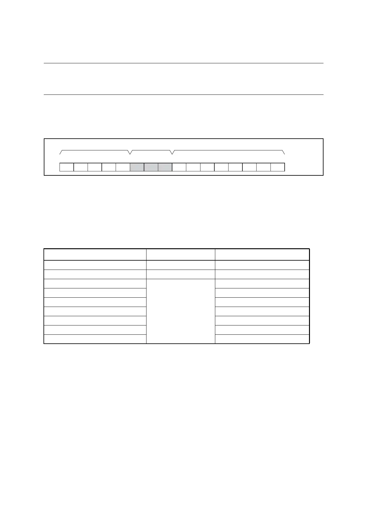
Figure 2.1-4 Configuration of Direct Bank Pointer
The area of "0x0000 to 0x007F" and that of "0x0090 to 0x047F" can be accessed by direct
addressing. Access to 0x0000 to 0x007F is specified by an operand regardless of the value in
the direct bank pointer. Access to 0x0090 to 0x047F is specified by the value of the direct bank
pointer and the operand.
Table 2.1-1 shows the relationship between the direct bank pointer (DP) and the access area;
Table 2.1-2 lists the direct addressing instructions.
*: The available access area varies among products. For details, refer to the device data sheet.
CCRDPRP
PS 0b000
DP
initial value
R4 R3 R2 R1 R0 DP2 DP1 DP0 H I IL1 IL0 N Z V C
bit15 bit14 bit13bit12 bit11 bit10 bit9 bit8bit7 bit6 bit5 bit4 bit3bit2 bit1 bit0
Table 2.1-1 Direct Bank Pointer and Access Area
Direct bank pointer (DP[2:0]) Operand-specified dir Access area*
0bXXX (It does not affect mapping.) 0x0000 to 0x007F 0x0000 to 0x007F
0b000 (Initial value) 0x0090 to 0x00FF 0x0090 to 0x00FF
0b001
0x0080 to 0x00FF
0x0100 to 0x017F
0b010 0x0180 to 0x01FF
0b011 0x0200 to 0x027F
0b100 0x0280 to 0x02FF
0b101 0x0300 to 0x037F
0b110 0x0380 to 0x03FF
0b111 0x0400 to 0x047F
 Loading...

