R8C/20 Group, R8C/21 Group 14. Timers
Rev.2.00 Aug 27, 2008 Page 179 of 458
REJ09B0250-0200
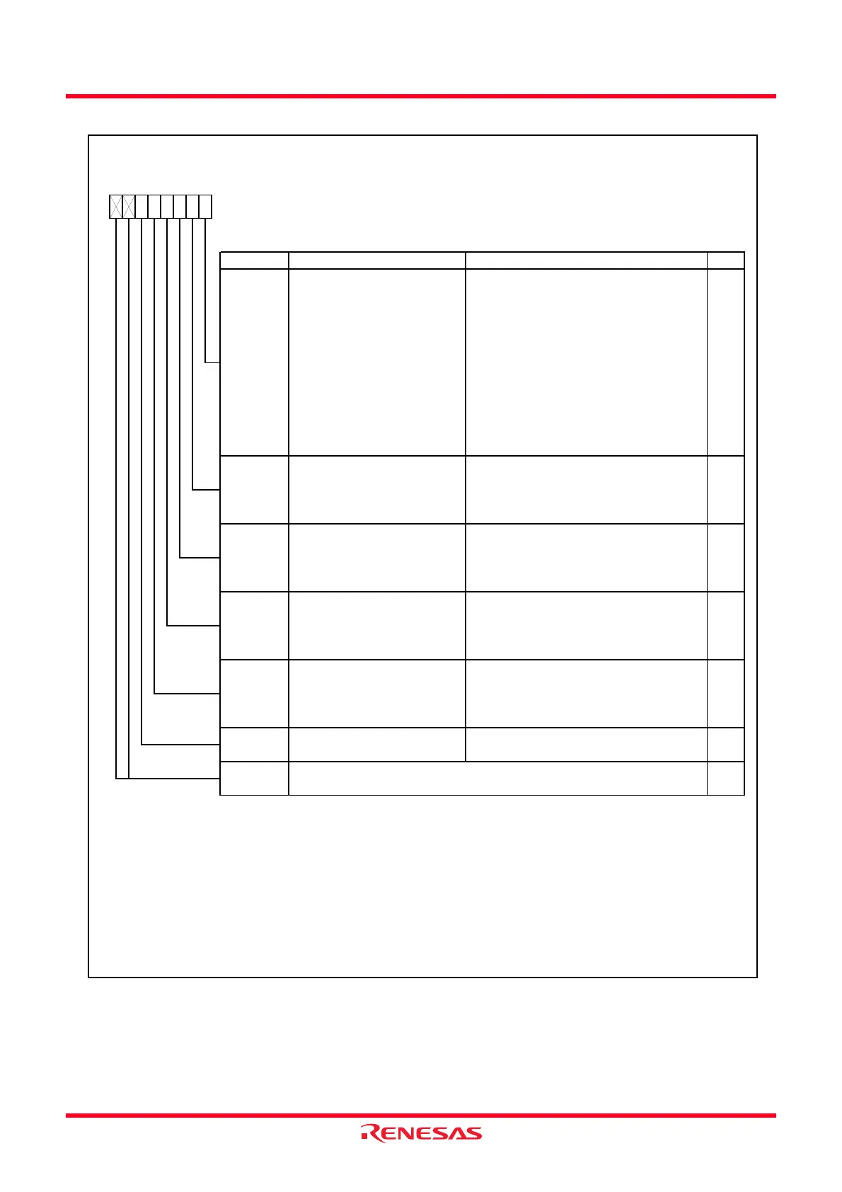
Figure 14.41 Registers TRDSR0 to TRDSR1 in Input Capture Function
Timer RD Status Register i (i = 0 or 1)
Symbol Address After Reset
TRDSR0
TRDSR1
0143h
0153h
11100000b
11000000b
Bit Symbol Bit Name Function RW
NOTES:
1.
2.
3.
4. Edge selected by bits IOk1 to IOk0 (k = C or D) in the TRDIORCi register.
Including w hen the BFki bit in the TRDMR register is set to 1 (TRDGRki is used as the buffer register).
Edge selected by bits IOj1 to IOj0 (j = A or B) in the TRDIORAi register.
The writing results are as follow s:
• This bit is set to 0 w hen the read result is 1 and w riting 0 to the same bit.
• This bit remains unchanged even if the read result is 0 and w riting 0 to the same bit. (This bit remains 1 even if this
bit is set to 1 from 0 after reading, and w riting 0.)
• This bit remains unchanged w hen w riting 1.
b3 b2
IMFD
b1 b0b7 b6 b5 b4
RW
IMFB RW
Input capture/compare match flag
A
[Source for setting this bit to 0]
Write 0 after read.
(2)
[Source for setting this bit to 1]
TRDSR0 register:
fOCO128 signal edge w hen the IOA3 bit in the
TRDIORA0 register is set to 0 (fOCO128
signal) TRDIOA0 pin input edge w hen the
IOA3 bit in the TRDIORA0 register is set to 1
(TRDIOA0 input)
(3)
TRDSR1 register:
Input edge of TRDIOA1 pin.
(3)
Input capture/compare match flag
B
[Source for setting this bit to 0]
Write 0 after read.
(2)
[Source for setting this bit to 1]
Input edge of TRDIOBi pin.
(3)
IMFA
Input capture/compare match flag
C
[Source for setting this bit to 0]
Write 0 after read.
(2)
[Source for setting this bit to 1]
Input edge of TRDIOCi pin.
(4)
Nothing is assigned to the b5 in the TRDSR0 register. When w riting to the b5, w rite 0. When reading, its content is 1.
IMFC RW
RW
Input capture/compare match flag
D
[Source for setting this bit to 0]
Write 0 after read.
(2)
[Source for setting this bit to 1]
Input edge of TRDIODi pin.
(4)
Overflow flag [Source for setting this bit to 0]
Write 0 after read.
(2)
[Source for setting this bit to 1]
When the TRDi register overflow s
—
(b7 - b6)
—
Nothing is assigned. If necessary, set to 0.
When read, the content is 1.
RWOVF
UDF
Underflow flag
(1)
This bit is disabled in the input capture
function.
RW
 Loading...