R8C/20 Group, R8C/21 Group 14. Timers
Rev.2.00 Aug 27, 2008 Page 243 of 458
REJ09B0250-0200
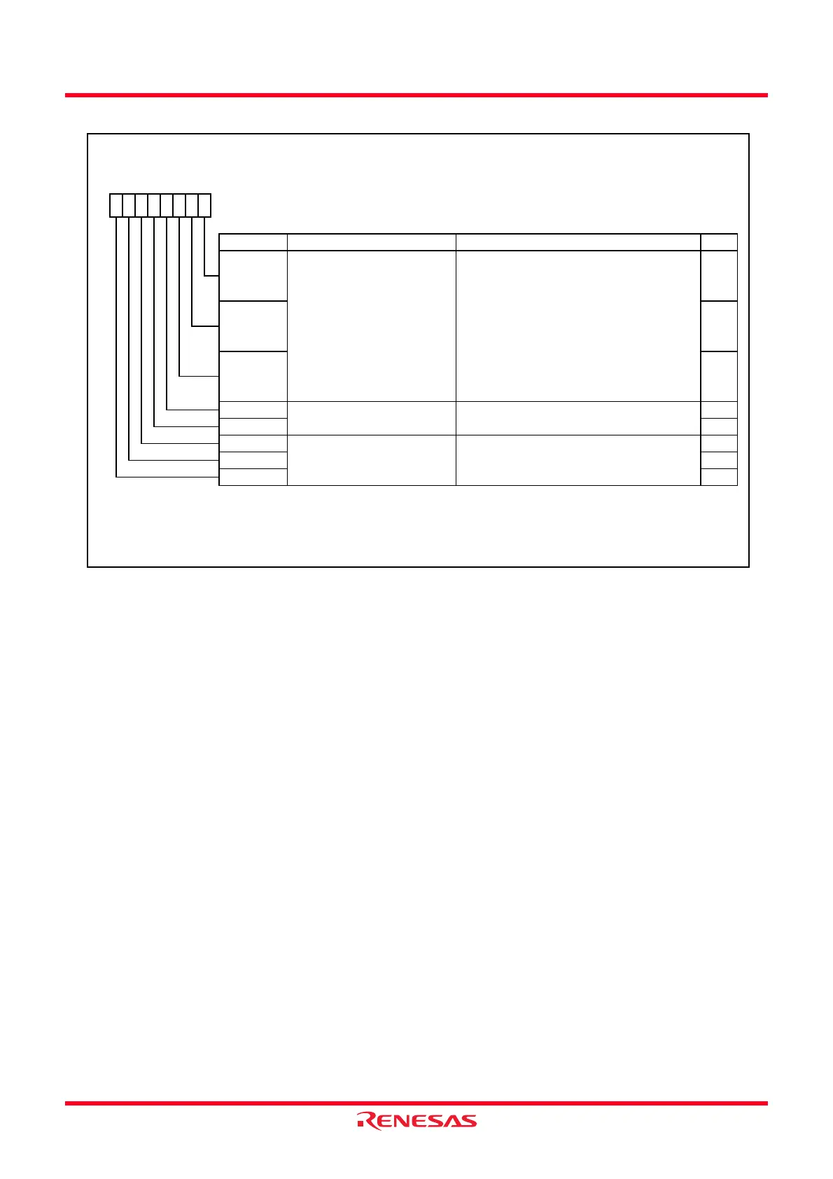
Figure 14.103 TRDCR0 Register in PWM3 Mode
Timer RD Control Register i (i = 0 or 1)
(2)
Symbol Address After Reset
TRDCR0
0140h 00h
Bit Symbol Bit Name Function RW
NOTES:
1.
2.
RW
TCK1 RW
TCK0
RW
RW
RW
CCLR2
CCLR1 RW
Count source selection bit
b2 b1b0
0 0 0 : f1
0 0 1 : f2
0 1 0 : f4
0 1 1 : f8
1 0 0 : f32
1 0 1 : Do not set
1 1 0 : fOCO40M
1 1 1 : Do not set
External clock edge selection
bit
(1)
This bit is disabled in PWM3 mode.
b7 b6 b5 b4
001
b3 b2
CKEG0
b1 b0
TCK2
The TRDCR1 register is not used in PWM3 mode.
RW
CKEG1
CCLR0 RWSet to 001b (the TRD0 register clear at the
compare match w ith TRDGRA0 register) in
PWM3 mode.
TRD0 counter clear selection bit
This bit is enabled w hen the TCK2 to TCK0 bits are set to 101b (TRDCLK input) and the STCLK bit in the TRDFCR
register is set to 1 (external clock input enabled).
 Loading...