R8C/20 Group, R8C/21 Group 14. Timers
Rev.2.00 Aug 27, 2008 Page 244 of 458
REJ09B0250-0200
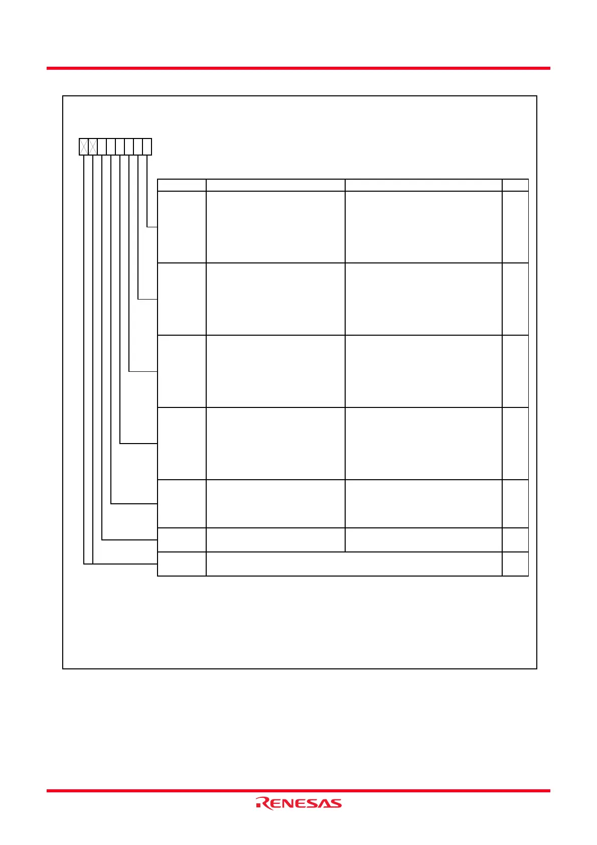
Figure 14.104 Registers TRDSR0 and TRDSR1 in PWM3 Mode
Timer RD Status Register i (i = 0 or 1)
Symbol Address After Reset
TRDSR0
0143h 11100000b
TRDSR1
0153h 11000000b
Bit Symbol Bit Name Function RW
NOTES:
1.
2.
b2
IMFD
b1 b0
RW
b7 b6 b5 b4 b3
RW
IMFB RW
Input capture/compare match flag A [Source for setting this bit to 0]
Write 0 after read.
(1)
[Source for setting this bit to 1]
When the value in the TRDi register
matches w ith the value in the TRDGRAi
register.
Input capture/compare match flag B [Source for setting this bit to 0]
Write 0 after read.
(1)
[Source for setting this bit to 1]
When the value in the TRDi register
matches w ith the value in the TRDGRBi
register.
IMFA
OVF
Input capture/compare match flag C [Source for setting this bit to 0]
Write 0 after read.
(1)
[Source for setting this bit to 1]
When the value in the TRDi register
matches w ith the value in the TRDGRCi
register.
(2)
IMFC
Overflow flag [Source for setting this bit to 0]
Write 0 after read.
(1)
[Source for setting this bit to 1]
When the TRDi register overflow s.
RW
RW
Input capture/compare match flag D [Source for setting this bit to 0]
Write 0 after read.
(1)
[Source for setting this bit to 1]
When the value in the TRDi register
matches w ith the value in the TRDGRDi
register.
(2)
Including w hen the BFji bit (j = C or D) in the TRDMR register is set to 1 (TRDGRji is used as the buffer register).
—
(b7 - b6)
—
Nothing is assigned. If necessary, set to 0.
When read, the content is 1.
The w riting results are as follow s:
• This bit is set to 0 w hen the read result is 1 and w riting 0 to the same bit.
• This bit remains unchanged even if the read result is 0 and w riting 0 to the same bit. (This bit remains 1 even if this
bit is set to 1 from 0 after reading, and w riting 0.)
• This bit remains unchanged w hen w riting 1.
UDF
Underflow flag
(1)
This bit is disabled in PWM3 mode.
RW
 Loading...