R8C/20 Group, R8C/21 Group 5. Resets
Rev.2.00 Aug 27, 2008 Page 23 of 458
REJ09B0250-0200
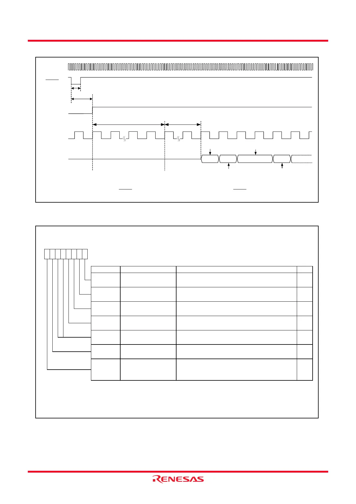
Figure 5.3 Reset Sequence
Figure 5.4 OFS Register
Start time of flash memory
(CPU clock × 14 cycles)
0FFFCh 0FFFEh
0FFFDh
Content of reset vector
CPU clock
Address
(internal address
signal)
NOTES:
1. Hardware reset.
2. When the “L” input width to the RESET pin is set to fOCO-S clock × 32 cycles or more, setting the RESET pin to “H” also sets the internal
reset signal to “H” at the same.
CPU clock × 28 cycles
fOCO-S clock × 32 cycles
(2)
fOCO-S
Internal reset
signal
RESET pin
10 cycles or more are needed
(1)
Option Function Select Register
(1)
Symbol Address Before Shipment
OFS
0FFFFh FFh
(3)
Bit Symbol Bit Name Function RW
Reserved bit
NOTES:
1.
2.
3.
b7 b6 b5 b4 b3 b2 b1 b0
11 1
—
(b1)
Set to 1
RW
WDTON
Watchdog timer start
select bit
0 : Starts w atchdog timer automatically after reset
1 : Watchdog timer is inactive after reset
RW
ROMCR
ROM code protect
disabled bit
0 : ROM code protect disabled
1 : ROMCP1 enabled
RW
ROMCP1
ROM code protect bit 0 : ROM code protect enabled
1 : ROM code protect disabled
RW
RW
—
(b5-b4)
Reserved bits Set to 1
RW
If the block including the OFS register is erased, FFh is set to the OFS register.
To use the pow er-on reset, set the LVD1ON bit to 0 (voltage monitor 1 reset enabled after reset).
LVD1ON
Voltage detection circuit
start bit
(2)
0 : Voltage monitor 1 reset enabled after reset
1 : Voltage monitor 1 reset disabled after reset
RW
The OFS register is on the flash memory. Write to the OFS register w ith a program. After w riting is completed, do not
w rite additions to the OFS register.
CSPROINI
Count source protect
mode after reset select
bit
0 : Count source protect mode enabled after reset
1 : Count source protect mode disabled after reset
 Loading...