RL78/G10 CHAPTER 6 TIMER ARRAY UNIT
R01UH0384EJ0311 Rev. 3.11 110
Dec 22, 2016
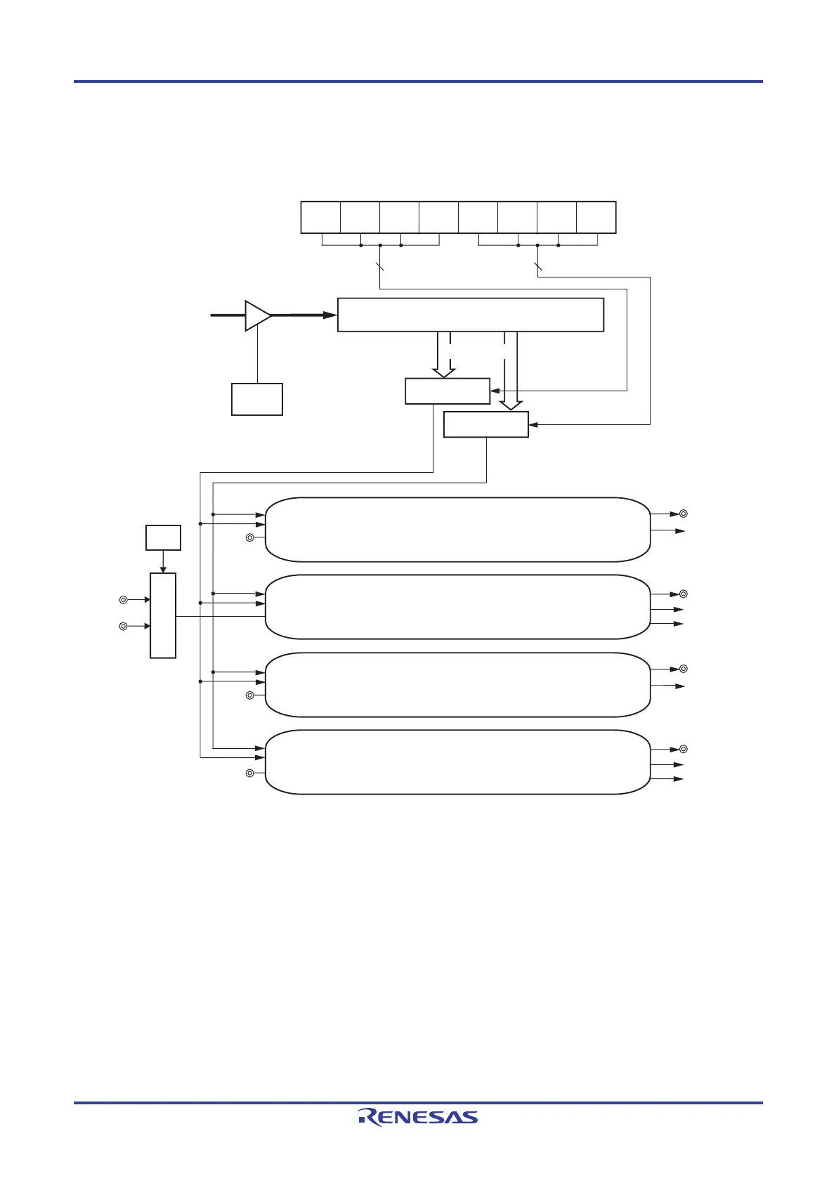
Figures 6-1 and 6-2 show the block diagrams of the timer array unit.
Figure 6-1. Entire Configuration of Timer Array Unit
TO01
TI00
TO00
INT
TM01
INTTM01H
f
CLK
f
CLK
/2 to f
CLK
/2
15
TAU0EN
TI02
TI03
CK00
CK01
Channel 0
Channel 1
Timer clock select register 0 (TPS0)
Peripheral enable
register 0
(PER0)
Selector
Selector
(Timer interrupt)
INTTM00
T
O03
TO02
INT
TMxx
INTTMxxH
Channel 2
Channel 3
(Timer interrupt)
INTTMxx
Prescaler
Note
Note
TI01
RxD0
Serial input pin
ISC
Input switch control
register (ISC)
Selector
4 4
PRS013 PRS003PRS012 PRS011 PRS010 PRS002 PRS001
PRS000
Note 16-pin products only.

 Loading...