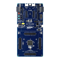
RL78/G10 CHAPTER 24 ELECTRICAL SPECIFICATIONS
R01UH0384EJ0311 Rev. 3.11 590
Dec 22, 2016
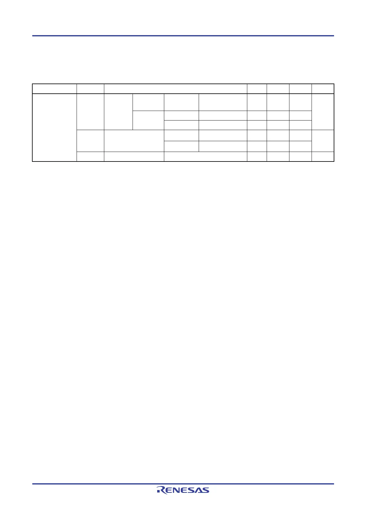
24.3.2 Supply current characteristics
(1) Flash ROM: 1 and 2 KB of 10-pin products
(TA = −40 to +85°C, 2.0 V ≤ VDD ≤ 5.5 V, VSS = 0 V)
Parameter Symbol Conditions MIN. TYP. MAX. Unit
Supply current
Note 1
I
DD1
Operating
mode
Basic
operation
f
IH = 20 MHz VDD = 3.0 V, 5.0 V 0.91 mA
Normal
operation
f
IH = 20 MHz VDD = 3.0 V, 5.0 V 1.57 2.04
fIH = 5 MHz VDD = 3.0 V, 5.0 V 0.85 1.15
IDD2
Note 2
HALT mode fIH = 20 MHz VDD = 3.0 V, 5.0 V 350 820 µA
fIH = 5 MHz VDD = 3.0 V, 5.0 V 290 600
IDD3
Note 3
STOP mode VDD = 3.0 V 0.56 2.00 µA
Notes 1. Total current flowing into VDD, including the input leakage current flowing when the level of the input pin is
fixed to VDD or VSS. The values below the MAX. column include the peripheral operation current. However,
not including the current flowing into the A/D converter, I/O port, and on-chip pull-up/pull-down resistors.
2. During HALT instruction execution by flash memory.
3. Not including the current flowing into the watchdog timer.
Remarks 1. f
IH: High-speed on-chip oscillator clock frequency
2. Temperature condition of the typical value is T
A = 25°C

 Loading...