RL78/G10 CHAPTER 2 PIN FUNCTIONS
R01UH0384EJ0311 Rev. 3.11 13
Dec 22, 2016
2.2.2 Description of functions
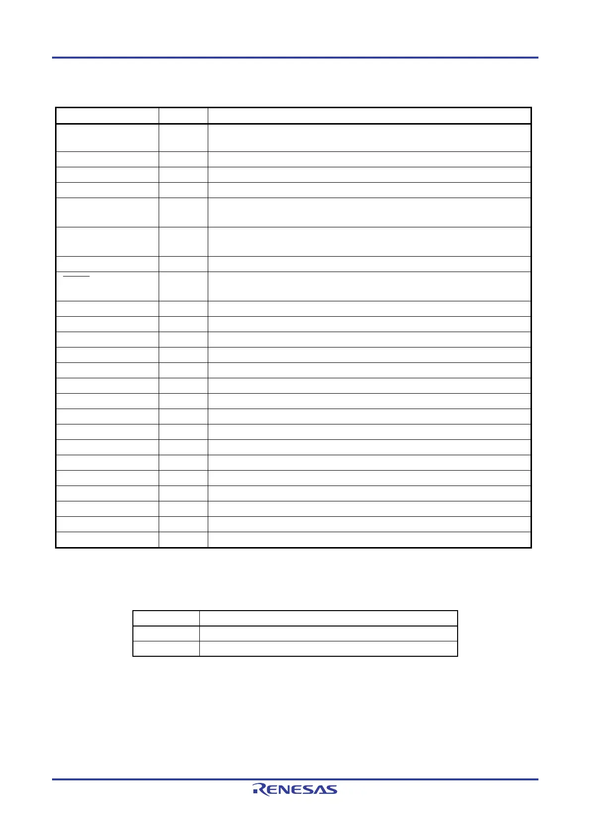
Function Name I/O Functions
ANI0 to ANI6 input
Analog input pins of A/D converter
(See Figure 10-23 Analog Input Pin Connection.)
IVCOUT0 output Comparator output
IVCMP0 input Analog input for the comparator
IVREF0 input Reference voltage input for the comparator
INTP0 to INTP3 input External interrupt request input
Specified available edge: Rising edge, falling edge, or both rising and falling edges
KR0 to KR5 input Key interrupt input
Specified available edge: Rising edge or falling edge
PCLBUZ0 output Clock/buzzer output
RESET input This is the active-low system reset input pin.
When the external reset pin is not used, connect this pin directly or via a resistor to V
DD.
RxD0 input Serial data input pin of serial interface UART0
TxD0 output Serial data output pin of serial interface UART0
SCK00, SCK01 I/O Serial clock I/O pins of serial interface CSI00 and CSI01
SI00, SI01 input Serial data input pins of serial interface CSI00 and CSI01
SO00, SO01 output Serial data output pins of serial interface CSI00 and CSI01
SCL00 output Serial clock output pin of serial interface simple I
2
C (IIC00)
SDA00 I/O Serial data I/O pin of serial interface simple I
2
C (IIC00)
SCLA0 I/O Clock I/O pin of serial interface IICA0
SDAA0 I/O Serial data I/O pin of serial interface IICA0
TI00 to TI03 input Inputting an external count clock/capture trigger to 16-bit timers 00 to 03
TO00 to TO03 output Timer output pins of 16-bit timers 00 to 03
X1, X2
−
Resonator connection for main system clock
EXCLK input External clock input for main system clock
VDD
−
Positive power supply
VSS
−
Ground potential
TOOL0 I/O Data I/O pin for a flash memory programmer/debugger
Caution After reset release, the relationships between P40/TOOL0 and the operating mode are as follows.
Table 2-1. Relationships Between P40/TOOL0 and Operation Mode After Reset Release
P40/TOOL0 Operating mode
VDD Normal operation mode
0 V Flash memory programming mode
For details, see 20.4.2 Flash memory programming mode.
Remark Use bypass capacitors (about 0.1
μ
F) as noise and latch up countermeasures with relatively thick wires at
the shortest distance to V
DD to VSS lines.

 Loading...