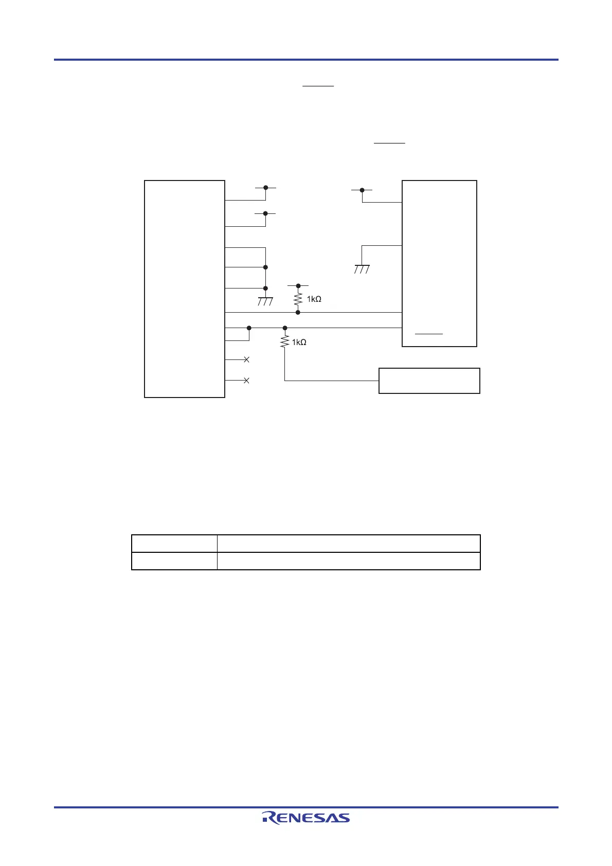
RL78/G10 CHAPTER 21 ON-CHIP DEBUG FUNCTION
R01UH0384EJ0311 Rev. 3.11 559
Dec 22, 2016
For the target system which uses the multi-use feature of RESET pin, its connection to an external circuit should be
isolated.
Figure 21-2. Connection Example of E1 On-chip Debugging Emulator and RL78 microcontroller
(When using to the alternative function of RESET pin)
V
DD
EMV
DD
GND
GND
GND
TOOL0
RSTPU
V
DD
V
DD
V
DD
V
DD
8
9
2
12
14
5
10
13
4
6
V
DD
V
SS
TOOL0
Alternate Function
of RESET pin
Output pin
E1 target connector
Reset_out
Reset_out
Reset_in
External circuit
RL78/G10
21.2 On-Chip Debug Security ID
The RL78 microcontroller has an on-chip debug operation control bit in the flash memory at 000C3H (see CHAPTER
19 OPTION BYTE) and an on-chip debug security ID setting area at 000C4H to 000CDH, to prevent third parties from
reading memory content.
Table 21-1. On-Chip Debug Security ID
Address On-Chip Debug Security ID
000C4H to 000CDH Any ID code of 10 bytes

 Loading...